
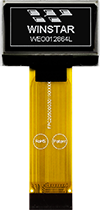
 - WEA012864L")
私たちはあなたのプライバシーを大切にします
「すべてのクッキーを許可」をクリックすると、サイトのナビゲーションを向上させ、サイト使用状況を分析し、マーケティングおよびパフォーマンスの取り組みを支援するために、クッキーをデバイスに保存することに同意したことになります。この件に関する詳細情報は、ポリシーをご覧ください。プライバシーポリシー


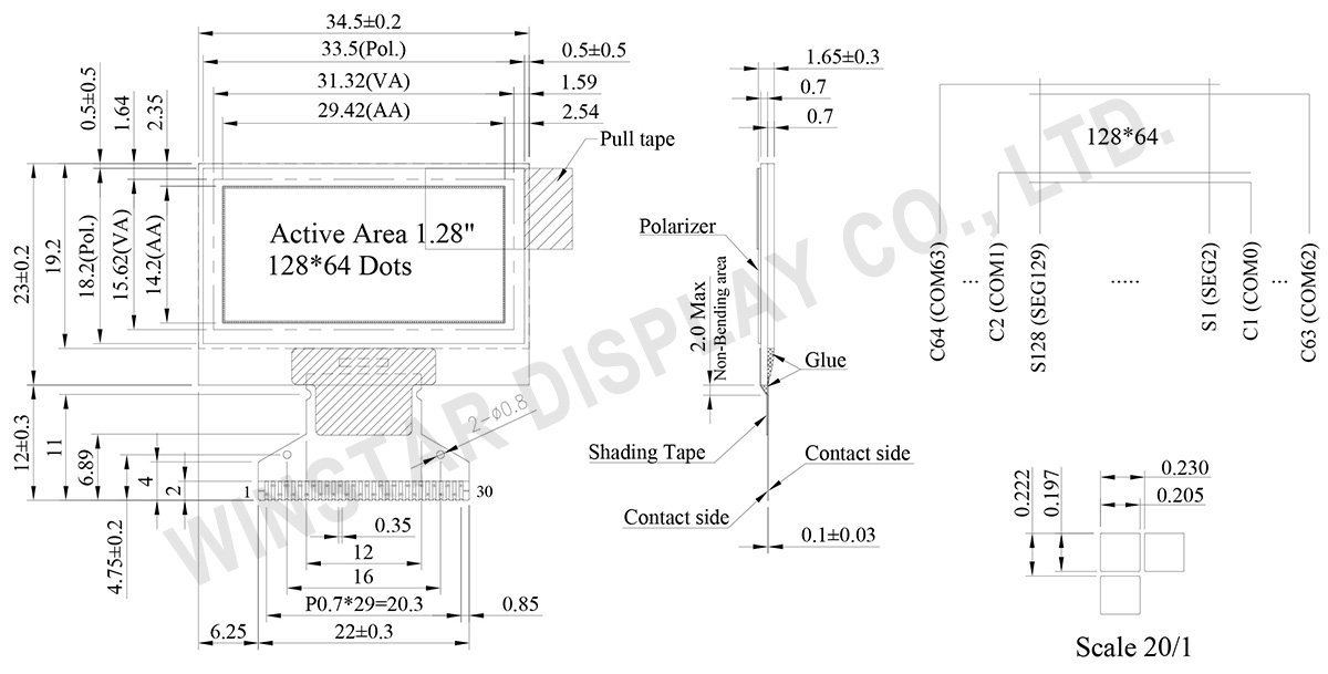
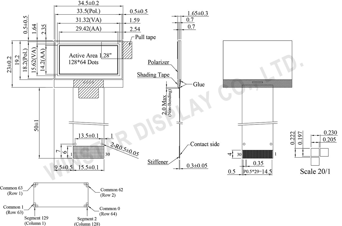
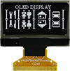
WEO012864L は 1.28" COG 構造のグラフィック OLED です。128x64 ドットの解像度で、製品の外径寸法は34.50x 23.00mmで、AA寸法は29.42x14.20mmです。SH1106 ICを内臓して、8bit 6800/8080/3線と4線のSPI/I2Cのインターフェースをサポート致します。3V駆動対応品です。お客様がアプリケーションに適したモジュールを選択できるように、ZIF FPC及びHotbarバージョンを提供しています。有機EL・COGモジュールは超薄、軽量、低消費電力のメリットを有して、ハンドヘルド機器、メーター、スマートグリッド、ウェアラブル機器、IoTシステムなどに生かせます。内部チャージポンプ電源と外部 VCC 電源をサポートしております。
 FPC Options
| 項目 | 標準値 | 単位 |
|---|---|---|
| ドットマトリックス(解像度) | 128 x 64 | - |
| 外形寸法 | 34.50 × 23.00 × 1.65 | mm |
| 有効表示エリア | 29.42 × 14.20 | mm |
| ドットサイズ | 0.205 × 0.197 | mm |
| ドットピッチ | 0.230 × 0.222 | mm |
| 表示モード | パッシブマトリクス | |
| 発光色 | モノクロ | |
| 駆動方法 | 1/64 Duty | |
| コントローラー IC | SH1106 | |
| インターフェイス | 6800/8080/3-SPI /4-SPI / I2C | |
| サイズ | 1.28 インチ | |
| パラメーター | 記号 | 最小値 | 最大値 | 単位 |
|---|---|---|---|---|
| ロジック電源電圧 | VDD1 | -0.3 | 3.6 | V |
| Power supply for charge pump circuit | VDD2 | -0.3 | 4.8 | V |
| Display電源電圧 | VPP | -0.3 | 14.5 | V |
| 操作温度 | TOP | -40 | +80 | °C |
| 保存温度 | TSTG | -40 | +85 | °C |
| 項目 | 記号 | 条件 | 最小値 | 典型値 | 最大値 | 単位 |
|---|---|---|---|---|---|---|
| ロジック電源電圧 | VDD1 | - | 2.8 | 3.0 | 3.3 | V |
| Display電源電圧 | VPP | - | 6.75 | 7.25 | 7.75 | V |
| 高レベル入力 | VIH | - | 0.8xVDD1 | - | VDD1 | V |
| 低レベル入力 | VIL | - | VSS | - | 0.2xVDD1 | V |
| 高レベル出力 | VOH | - | 0.8xVDD1 | - | VDD1 | V |
| 低レベル出力 | VOL | - | VSS | - | 0.2xVDD1 | V |
| Display 50% Pixel on | IPP | VPP =7.25V | - | 6.0 | 9.0 | mA |
| No. | 記号 | 説明 | ||||||||||||||||||||||||
|---|---|---|---|---|---|---|---|---|---|---|---|---|---|---|---|---|---|---|---|---|---|---|---|---|---|---|
| 1 | NC(GND) | No connection | ||||||||||||||||||||||||
| 2 | C1N | Connect to charge pump capacitor. These pins are not used and should be disconnected when Vpp is supplied externally. |
||||||||||||||||||||||||
| 3 | C1P | |||||||||||||||||||||||||
| 4 | C2P | Connect to charge pump capacitor. These pins are not used and should be disconnected when Vpp is supplied externally. |
||||||||||||||||||||||||
| 5 | C2N | |||||||||||||||||||||||||
| 6 | VDD2 | 3.0 – 4.7V power supply pad for Power supply for charge pump circuit. This pin should be disconnected when VPP is supplied externally |
||||||||||||||||||||||||
| 7 | NC | No connection | ||||||||||||||||||||||||
| 8 | VSS | Ground. | ||||||||||||||||||||||||
| 9 | VDD1 | Power supply input: 1.65 - 3.5V | ||||||||||||||||||||||||
| 10 | IM0 | These are the MPU interface mode select pads.
|
||||||||||||||||||||||||
| 11 | IM1 | |||||||||||||||||||||||||
| 12 | IM2 | |||||||||||||||||||||||||
| 13 | CSB | This pad is the chip select input. When CSB = “L”, then the chip select becomes active, and data/command I/O is enabled. | ||||||||||||||||||||||||
| 14 | RESB | This is a reset signal input pad. When RES is set to “L”, the settings are initialized. The reset operation is performed by the RES signal level. | ||||||||||||||||||||||||
| 15 | A0 | This is the Data/Command control pad that determines whether the data bits are data or a command. A0 = “H”: the inputs at D0 to D7 are treated as display data. A0 = “L”: the inputs at D0 to D7 are transferred to the command registers. In I2C interface, this pad serves as SA0 to distinguish the different address of OLED driver. |
||||||||||||||||||||||||
| 16 | WRB | This is a MPU interface input pad. When connected to an 8080 MPU, this is active LOW. This pad connects to the 8080 MPU WR signal. The signals on the data bus are latched at the rising edge of the WR signal. When connected to a 6800 Series MPU: This is the read/write control signal input terminal. When R/W = “H”: Read. When R/W = “L”: Write. |
||||||||||||||||||||||||
| 17 | RDB | This is a MPU interface input pad. When connected to an 8080 series MPU, it is active LOW. This pad is connected to the RD signal of the 8080 series MPU, and the data bus is in an output status when this signal is “L”. When connected to a 6800 series MPU , this is active HIGH. This is used as an enable clock input of the 6800 series MPU. When RD = “H”: Enable. When RD = “L”: Disable. |
||||||||||||||||||||||||
| 18 | D0 | This is an 8-bit bi-directional data bus that connects to an 8-bit or 16-bit standard MPU data bus. When the serial interface is selected, then D0 serves as the serial clock input pad (SCL) and D1 serves as the serial data input pad (SI). At this time, D2 to D7 are set to high impedance. When the I2C interface is selected, then D0 serves as the serial clock input pad (SCL) and D1 serves as the serial data input pad (SDAI). At this time, D2 to D7 are set to high impedance. |
||||||||||||||||||||||||
| 19 | D1 | |||||||||||||||||||||||||
| 20 | D2 | |||||||||||||||||||||||||
| 21 | D3 | |||||||||||||||||||||||||
| 22 | D4 | |||||||||||||||||||||||||
| 23 | D5 | |||||||||||||||||||||||||
| 24 | D6 | |||||||||||||||||||||||||
| 25 | D7 | |||||||||||||||||||||||||
| 26 | IREF | This is a segment current reference pad. A resistor should be connected between this pad and VSS. Set the current at 18.75uA. | ||||||||||||||||||||||||
| 27 | VCOMH | This is a pad for the voltage output high level for common signals. A capacitor should be connected between this pad and VSS. |
||||||||||||||||||||||||
| 28 | VPP | OLED panel power supply. Generated by internal charge pump. Connect to capacitor. It could be supplied externally. |
||||||||||||||||||||||||
| 29 | VSL | This is a segment voltage reference pad. This pad should be connected to VSS externally. |
||||||||||||||||||||||||
| 30 | NC(GND) | No connection |
| Drawing | FPC Length | PIN | Pitch | ZIF FPC or HOTBAR FPC | Interface | FPC No. | Create Date |
|---|---|---|---|---|---|---|---|
 |
13.2 | 30 | 0.7 | HOTBAR FPC | 6800/8080/3-SPI /4-SPI / I2C | FPC2070003001XXXXX03 | 20141107 |
 |
51.15 | 30 | 0.5 | ZIF | 6800/8080/3-SPI /4-SPI / I2C | FPC2050003011XXXXX18 | 20180123 |

「すべてのクッキーを許可」をクリックすると、サイトのナビゲーションを向上させ、サイト使用状況を分析し、マーケティングおよびパフォーマンスの取り組みを支援するために、クッキーをデバイスに保存することに同意したことになります。この件に関する詳細情報は、ポリシーをご覧ください。プライバシーポリシー