


 - WEX025664B-CTP")


私たちはあなたのプライバシーを大切にします
「すべてのクッキーを許可」をクリックすると、サイトのナビゲーションを向上させ、サイト使用状況を分析し、マーケティングおよびパフォーマンスの取り組みを支援するために、クッキーをデバイスに保存することに同意したことになります。この件に関する詳細情報は、ポリシーをご覧ください。プライバシーポリシー


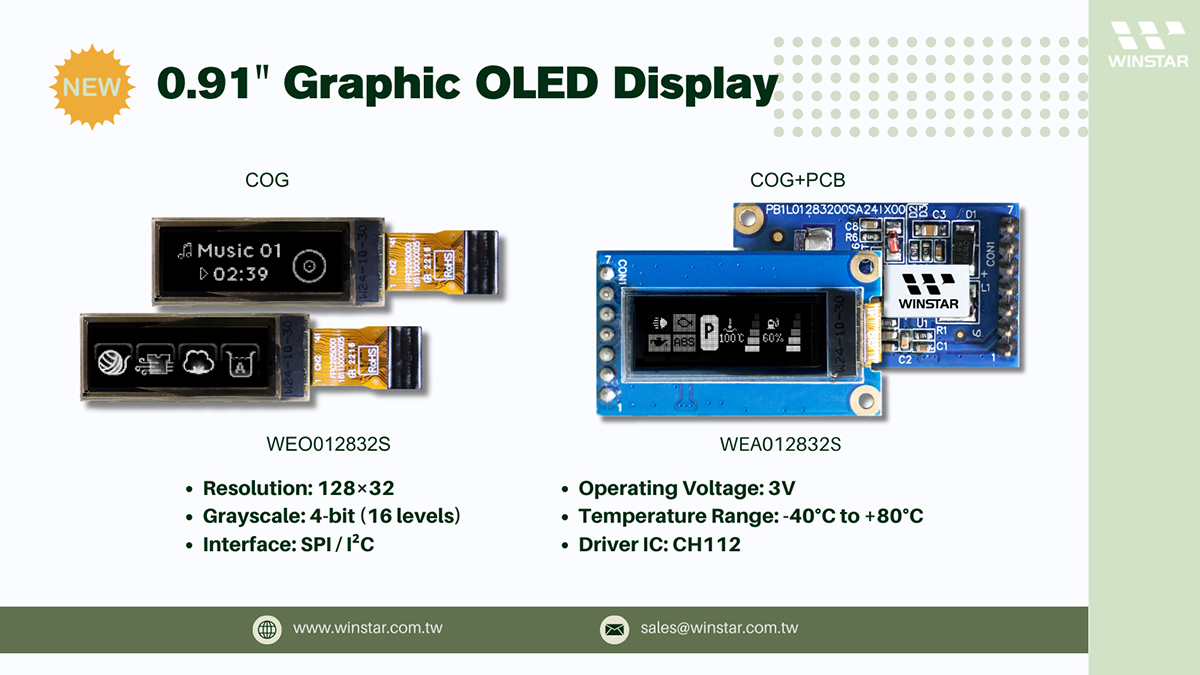
WEO012832S は 0.91インチOLEDディスプレイ モジュールで、128x32ドットマトリックス と統合された CH1120ドライバーIC を備えています。コンパクトなシステム向けに設計されており、この0.91インチOLEDディスプレイ は、機械的な奥行き、電力効率、そして明瞭なモノクロ表示が重要な制約となるアプリケーションに最適化されています。4ビットグレースケールに対応しており、従来の1ビットOLEDモジュールに比べて、UI表現の柔軟性が向上しています。詳細な仕様については、OLED 0.91"データシート をご参照ください。
OLEDディスプレイ 0.91 128x32 は、3Vのロジック電源で動作し、SPIおよびI2Cインターフェースを提供しており、ほとんどのMCUプラットフォームとのシームレスな統合が可能です。モジュールは、160°(水平/垂直)の広視野角を持ち、-40°Cから+80°Cまでの広範囲な動作温度範囲を提供し、消費者および産業環境の両方で安定したパフォーマンスを保証します。
もしプロジェクトに追加の機械的サポート、簡便な取り付け、または迅速なプロトタイピングが必要であれば、同じディスプレイが COG+PCB バージョンとしても提供されています。
PCB 統合型の構成については WEA012832S を参照してください。
Data source ref:WEO012832SWPP3N00000
| 項目 | 仕様 | 単位 |
|---|---|---|
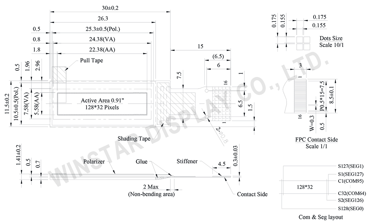
| ドットマトリックス | 128 × 32 Dots | - |
| モジュールサイズ | 30.0 × 11.5 × 1.41 | mm |
| 有効エリア | 22.38 × 5.58 | mm |
| ピクセルサイズ | 0.155 × 0.155 | mm |
| ピクセルピッチ | 0.175 × 0.175 | mm |
| 表示モード | パッシブマトリクス(Passive Matrix) | |
| 発光色 | モノクロ | |
| 駆動方法 | 1/32 Duty | |
| グレースケール | 4 bits | |
| IC | CH1120 | |
| インターフェイス | 4-wire SPI,I2C | |
| サイズ (対角線) | 0.91 インチ | |
| パラメーター | 記号 | 最小値 | 最大値 | 単位 |
|---|---|---|---|---|
| ロジック電源電圧 | VDD | -0.3 | 3.5 | V |
| ディスプレイの供給電圧 | VPP | -0.3 | 15.0 | V |
| 操作温度 | TOP | -40 | +80 | °C |
| 保存温度 | TSTG | -40 | +85 | °C |
| 項目 | 記号 | 条件 | 最小値 | 典型値 | 最大値 | 単位 |
|---|---|---|---|---|---|---|
| ロジック電源電圧 | VDD | - | 1.65 | 3.0 | 3.5 | V |
| ディスプレイの供給電圧 | VPP | - | 8.0 | 9.0 | 9.5 | V |
| 高レベル入力 | VIH | - | 0.8×VDD | - | VDD | V |
| 低レベル入力 | VIL | - | VSS | - | 0.2×VDD | V |
| 高レベル出力 | VOH | - | 0.8×VDD | - | VDD | V |
| 低レベル出力 | VOL | - | VSS | - | 0.2×VDD | V |
| ディスプレイの50%ピクセル点灯時 | IPP | VPP=9V | - | 3 | 6 | mA |
| No. | 記号 | 功能説明 | ||||||
|---|---|---|---|---|---|---|---|---|
| 1 | ESD_GND | This pin should be connected to GND. | ||||||
| 2 | VPP | OLED panel power supply. Connect to capacitor. It could be supplied externally. This is the most positive voltage supply. |
||||||
| 3 | VCOMH | This is a pin for the voltage output high level for common signals. A capacitor should be connected between this pin and VSS. |
||||||
| 4 | SEGH | This is a segment pre-charge voltage. A capacitor can be connected between this pin and GND if necessary. When external capacitor is not used, this pin should be kept NC. |
||||||
| 5 | VSL | Discharge voltage level pad. This pad should be connected to resistor and diode externally. |
||||||
| 6 | VSS | Ground for logic and analog. This pin should be connected to GND externally. | ||||||
| 7 | VDD | Power supply for logic. | ||||||
| 8 | RES | This is a reset signal input pin. When RES is set to “L”, the settings are initialized. The reset operation is performed by the RES signal level. This pin internal pull high. |
||||||
| 9 | A0/SA0 | This is the Data/Command control pin that determines whether the data bits are data or a command. In I2C interface, this pad serves as SA0 to distinguish the different address of OLED driver. |
||||||
| 10 | CS | This pin is the chip select input. When CS = “L”, then the chip select becomes active, and data/command I/O is enabled. | ||||||
| 11 | SCL | The serial clock input. | ||||||
| 12 | SI | The serial data input. | ||||||
| 13 | IM1 | MCU bus interface selection pins.
|
||||||
| 14 | IREF | This is a segment current reference pin. A resistor should be connected between this pin and GND. |
||||||
| 15 | DVDD | This pin is for regulator circuit. A capacitor should be connected between this pin and GND if necessary. When external capacitor Is not used, this pin should be kept NC |
||||||
| 16 | ESD_GND | This pin should be connected to GND. |

「すべてのクッキーを許可」をクリックすると、サイトのナビゲーションを向上させ、サイト使用状況を分析し、マーケティングおよびパフォーマンスの取り組みを支援するために、クッキーをデバイスに保存することに同意したことになります。この件に関する詳細情報は、ポリシーをご覧ください。プライバシーポリシー