私たちはあなたのプライバシーを大切にします
「すべてのクッキーを許可」をクリックすると、サイトのナビゲーションを向上させ、サイト使用状況を分析し、マーケティングおよびパフォーマンスの取り組みを支援するために、クッキーをデバイスに保存することに同意したことになります。この件に関する詳細情報は、ポリシーをご覧ください。プライバシーポリシー


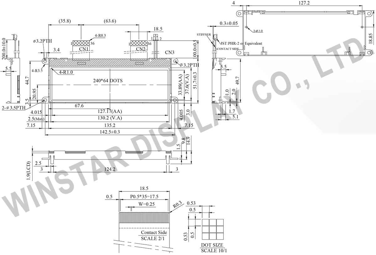
WO24064A1は、5.18インチ 240x64ドット モノクロCOGグラフィックLCDモジュールです。ST7565PコントローラICを搭載し、6800、8080および4-Line SPIインターフェースに対応しています。ロジック電源電圧は3.3Vです。
モジュールサイズは142.5 x 51.7 x 14.9 mm、表示エリア(VA)は130.2 x 37.6 mm、有効表示エリア(AA)は127.17 x 33.89 mmです。LCDタイプとLEDバックライトカラーは、複数の組み合わせから選択できます。ページ上部のお問い合わせに追加をクリックし、お問い合わせ内容にご希望の仕様をご記入ください。
産業機器、計測機器、医療機器、自動化システム、および各種組み込みHMI機器に適しています。
| 項目 | 標準値 | 単位 |
|---|---|---|
| 表示ドット数 | 240 x 64 | - |
| モジュールサイズ | 142.5 x 51.7 x 14.9(MAX) | mm |
| 表示エリア | 130.2 x 37.6 | mm |
| 有効エリア | 127.17 x 33.89 | mm |
| ドットサイズ | 0.50 x 0.50 | mm |
| ドットピッチ | 0.53 x 0.53 | mm |
| 駆動方法 | 1/65 | |
| バックライトタイプ | LED | |
| IC | ST7565P | |
| インターフェイス | 6800/8080/4-Line SPI | |
| 項目 | 記号 | 最小値 | 典型値 | 最大値 | 単位 |
|---|---|---|---|---|---|
| 操作温度 | TOP | -20 | - | +70 | ℃ |
| 保存温度 | TST | -30 | - | +80 | ℃ |
| 電源電圧 | VDD | -0.3 | - | 3.6 | V |
| Power supply voltage (VDD standard) | V0,VOUT | -0.3 | - | 14.5 | V |
| Power supply voltage (VDD standard) | V1,V2,V3,V4 | -0.3 | - | V0+0.3 | V |
| 項目 | 記号 | 条件 | 最小値 | 典型値 | 最大値 | 単位 |
|---|---|---|---|---|---|---|
| ロジック電源電圧 | VDD-VSS | - | 3.0 | 3.3 | 3.6 | V |
| LCM供給電圧 | V0-VSS | Ta=-20℃ Ta=25℃ Ta=70℃ |
- 10. - |
- 11.0 - |
- 11.3 - |
V V V |
| 高レベル入力電圧 | VIH | - | 0.8 VDD | - | VDD | V |
| 低レベル入力電圧 | VIL | - | VSS | - | 0.2VDD | V |
| 高レベル出力電圧 | VOH | - | 0.8VDD | - | VDD | V |
| 低レベル出力電圧 | VOL | - | VSS | - | 0.2VDD | V |
| 供給電流 | IDD | VDD=3.3V | - | 1.5 | 2.5 | mA |
| Pin No. | 記号 | Level | 説明 |
|---|---|---|---|
| 1 | NC | No connection | |
| 2 | FR | O | This is the liquid crystal alternating current signal terminal. |
| 3 | CL | I/O | This is the display clock input terminal The following is true depending on the M/S and CLS status. |
| 4 | /DOF | O | This is the LCD blanking control terminal. |
| 5 | /CS1 | I | This is the chip select signal. When /CS1 = “L” and CS2 = “H”, then the chip Select becomes active, and data/command I/O is enabled. |
| 6 | CS2 | I | |
| 7 | /RES | I | When /RES is set to “L”, the register settings are initialized (cleared). The reset operation is performed by the /RES signal level. |
| 8 | A0 | I | This is connect to the least significant bit of the normal MPU address bus, and it determines whether the data bits are data or command. A0 = “H”: Indicates that D0 to D7 are display data. A0 = “L”: Indicates that D0 to D7 are control data. |
| 9 | /WR | I | When connected to 8080 series MPU, this pin is treated as the “/WR” signal of the 8080 MPU and is LOW-active. The signals on the data bus are latched at the rising edge of the /WR signal. When connected to 6800 series MPU, this pin is treated as the “R/W” signal of the 6800 MPU and decides the access type : When R/W = “H”: Read. When R/W = “L”: Write. |
| 10 | /RD | I | When connected to 8080 series MPU, this pin is treated as the “/RD” signal of the 8080 MPU and is LOW-active. The data bus is in an output status when this signal is “L”. When connected to 6800 series MPU, this pin is treated as the “E” signal of the 6800 MPU and is HIGH-active. This is the enable clock input terminal of the 6800 Series MPU. |
| 11~18 | DB0~DB7 | I/O | Data bus |
| 19 | VDD | P | Power supply |
| 20 | VSS | P | Ground |
| 21 | Vout | O | DC/DC voltage converter. Connect a capacitor between this terminal and VSS or VDD |
| 22 | C3+ | O | DC/DC voltage converter |
| 23 | C1- | ||
| 24 | C1+ | ||
| 25 | C2+ | ||
| 26 | C2- | ||
27 |
V4 | P | This is a multi-level power supply for the liquid crystal drive. The voltage Supply applied is determined by the liquid crystal cell, and is changed through the use of a resistive voltage divided or through changing the impedance using an op. amp. Voltage levels are determined based on Vss, and must maintain the relative magnitudes shown below. V0 ≧V1 ≧V2 ≧V3 ≧V4 ≧Vss |
| 28 | V3 | ||
| 29 | V2 | ||
| 30 | V1 | ||
| 31 | V0 | ||
| 32 | VR | I | Output voltage regulator terminal. Provides the voltage between VSS and V0 through a resistive voltage divider. IRS = “L” : the V0 voltage regulator internal resistors are not used. IRS = “H” : the V0 voltage regulator internal resistors are used. |
| 33 | C86 | I | This is the MPU interface selection pin. C86 = “H”: 6800 Series MPU interface. C86 = “L”: 8080 Series MPU interface. |
| 34 | P/S | I | This pin configures the interface to be parallel mode or serial mode. P/S = “H”: Parallel data input/output. P/S = “L”: Serial data input. The following applies depending on the P/S status: P/S Data/Command Data Read/Write Serial Clock “H” A0 D0 to D7 /RD, /WR X “L” A0 SI (D7) Write only SCL (D6) When P/S = “L”, D0 to D5 must be fixed to “H”. /RD (E) and /WR (R/W) are fixed to either “H” or “L”. The serial access mode does NOT support read operation. |
| 35 | NC | No connection | |
| 36 | NC | No connection |

「すべてのクッキーを許可」をクリックすると、サイトのナビゲーションを向上させ、サイト使用状況を分析し、マーケティングおよびパフォーマンスの取り組みを支援するために、クッキーをデバイスに保存することに同意したことになります。この件に関する詳細情報は、ポリシーをご覧ください。プライバシーポリシー