我們重視您的隱私
通過點擊「允許所有 Cookie」,代表您同意在您的設備上存儲 Cookie 以增強網站瀏覽體驗、分析網站使用情況並協助我們的行銷和網站效能優化工作。您可以在我們的隱私權政策中找到有關於此的更多資訊。


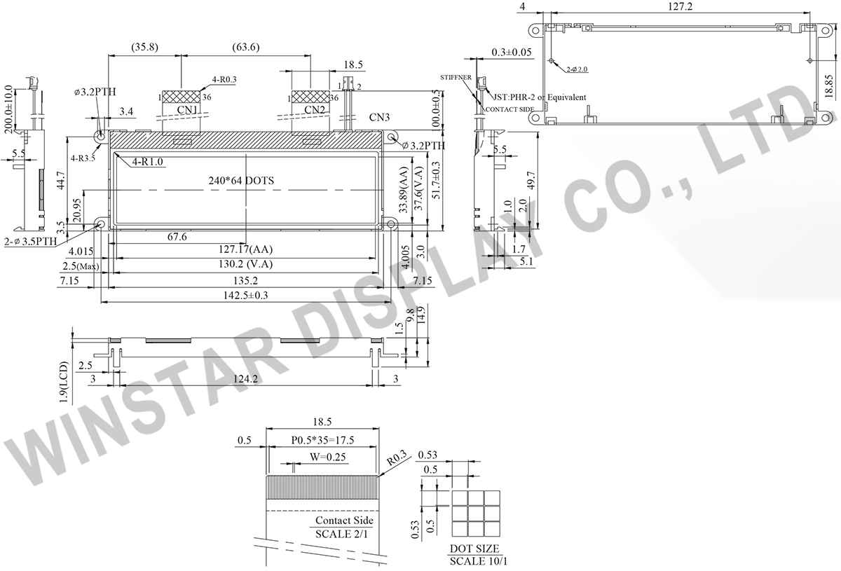
WO24064A1 為一款 5.18 吋 240x64 單色圖形 COG LCD 液晶顯示器,搭載 ST7565P 控制器,支援 6800、8080 與 4-Line SPI 介面,採用 3.3V 邏輯電源。
模組尺寸為 142.5 x 51.7 x 14.9 mm,檢視區域為 130.2 x 37.6 mm,有效區域為 127.17 x 33.89 mm。另有多種 LCD 類型與 LED 背光顏色組合可供選擇。請點選上方的『產品詢問』,並於詢問內容中註明所需規格。
適用於工業設備、量測儀器、醫療設備、自動化控制系統及各類嵌入式 HMI 應用。
| 項目 | 標準尺寸 | 單位 |
|---|---|---|
| 點陣數 | 240 x 64 | - |
| 模組尺寸 | 142.5 x 51.7 x 14.9(MAX) | mm |
| 檢視區域 | 130.2 x 37.6 | mm |
| 有效區域 | 127.17 x 33.89 | mm |
| 點大小 | 0.50 x 0.50 | mm |
| 點間距 | 0.53 x 0.53 | mm |
| 驅動方式 | 1/65 | |
| 背光類型 | LED | |
| IC | ST7565P | |
| 介面 | 6800/8080/4-Line SPI | |
| 項目 | 符號 | 最小值 | 典型值 | 最大值 | 單位 |
|---|---|---|---|---|---|
| 工作溫度 | TOP | -20 | - | +70 | ℃ |
| 儲存溫度 | TST | -30 | - | +80 | ℃ |
| 電源電壓 | VDD | -0.3 | - | 3.6 | V |
| Power supply voltage (VDD standard) | V0,VOUT | -0.3 | - | 14.5 | V |
| Power supply voltage (VDD standard) | V1,V2,V3,V4 | -0.3 | - | V0+0.3 | V |
| 項目 | 符號 | 條件 | 最小值 | 典型值 | 最大值 | 單位 |
|---|---|---|---|---|---|---|
| 邏輯電源電壓 | VDD-VSS | - | 3.0 | 3.3 | 3.6 | V |
| LCM電源電壓 | V0-VSS | Ta=-20℃ Ta=25℃ Ta=70℃ |
- 10. - |
- 11.0 - |
- 11.3 - |
V V V |
| 輸入高電壓 | VIH | - | 0.8 VDD | - | VDD | V |
| 輸入低電壓 | VIL | - | VSS | - | 0.2VDD | V |
| 輸出高電壓 | VOH | - | 0.8VDD | - | VDD | V |
| 輸出低電壓 | VOL | - | VSS | - | 0.2VDD | V |
| 電源電流(不包括LED背光) | IDD | VDD=3.3V | - | 1.5 | 2.5 | mA |
| Pin No. | 符號 | Level | 說明 |
|---|---|---|---|
| 1 | NC | No connection | |
| 2 | FR | O | This is the liquid crystal alternating current signal terminal. |
| 3 | CL | I/O | This is the display clock input terminal The following is true depending on the M/S and CLS status. |
| 4 | /DOF | O | This is the LCD blanking control terminal. |
| 5 | /CS1 | I | This is the chip select signal. When /CS1 = “L” and CS2 = “H”, then the chip Select becomes active, and data/command I/O is enabled. |
| 6 | CS2 | I | |
| 7 | /RES | I | When /RES is set to “L”, the register settings are initialized (cleared). The reset operation is performed by the /RES signal level. |
| 8 | A0 | I | This is connect to the least significant bit of the normal MPU address bus, and it determines whether the data bits are data or command. A0 = “H”: Indicates that D0 to D7 are display data. A0 = “L”: Indicates that D0 to D7 are control data. |
| 9 | /WR | I | When connected to 8080 series MPU, this pin is treated as the “/WR” signal of the 8080 MPU and is LOW-active. The signals on the data bus are latched at the rising edge of the /WR signal. When connected to 6800 series MPU, this pin is treated as the “R/W” signal of the 6800 MPU and decides the access type : When R/W = “H”: Read. When R/W = “L”: Write. |
| 10 | /RD | I | When connected to 8080 series MPU, this pin is treated as the “/RD” signal of the 8080 MPU and is LOW-active. The data bus is in an output status when this signal is “L”. When connected to 6800 series MPU, this pin is treated as the “E” signal of the 6800 MPU and is HIGH-active. This is the enable clock input terminal of the 6800 Series MPU. |
| 11~18 | DB0~DB7 | I/O | Data bus |
| 19 | VDD | P | Power supply |
| 20 | VSS | P | Ground |
| 21 | Vout | O | DC/DC voltage converter. Connect a capacitor between this terminal and VSS or VDD |
| 22 | C3+ | O | DC/DC voltage converter |
| 23 | C1- | ||
| 24 | C1+ | ||
| 25 | C2+ | ||
| 26 | C2- | ||
27 |
V4 | P | This is a multi-level power supply for the liquid crystal drive. The voltage Supply applied is determined by the liquid crystal cell, and is changed through the use of a resistive voltage divided or through changing the impedance using an op. amp. Voltage levels are determined based on Vss, and must maintain the relative magnitudes shown below. V0 ≧V1 ≧V2 ≧V3 ≧V4 ≧Vss |
| 28 | V3 | ||
| 29 | V2 | ||
| 30 | V1 | ||
| 31 | V0 | ||
| 32 | VR | I | Output voltage regulator terminal. Provides the voltage between VSS and V0 through a resistive voltage divider. IRS = “L” : the V0 voltage regulator internal resistors are not used. IRS = “H” : the V0 voltage regulator internal resistors are used. |
| 33 | C86 | I | This is the MPU interface selection pin. C86 = “H”: 6800 Series MPU interface. C86 = “L”: 8080 Series MPU interface. |
| 34 | P/S | I | This pin configures the interface to be parallel mode or serial mode. P/S = “H”: Parallel data input/output. P/S = “L”: Serial data input. The following applies depending on the P/S status: P/S Data/Command Data Read/Write Serial Clock “H” A0 D0 to D7 /RD, /WR X “L” A0 SI (D7) Write only SCL (D6) When P/S = “L”, D0 to D5 must be fixed to “H”. /RD (E) and /WR (R/W) are fixed to either “H” or “L”. The serial access mode does NOT support read operation. |
| 35 | NC | No connection | |
| 36 | NC | No connection |

通過點擊「允許所有 Cookie」,代表您同意在您的設備上存儲 Cookie 以增強網站瀏覽體驗、分析網站使用情況並協助我們的行銷和網站效能優化工作。您可以在我們的隱私權政策中找到有關於此的更多資訊。