私たちはあなたのプライバシーを大切にします
「すべてのクッキーを許可」をクリックすると、サイトのナビゲーションを向上させ、サイト使用状況を分析し、マーケティングおよびパフォーマンスの取り組みを支援するために、クッキーをデバイスに保存することに同意したことになります。この件に関する詳細情報は、ポリシーをご覧ください。プライバシーポリシー

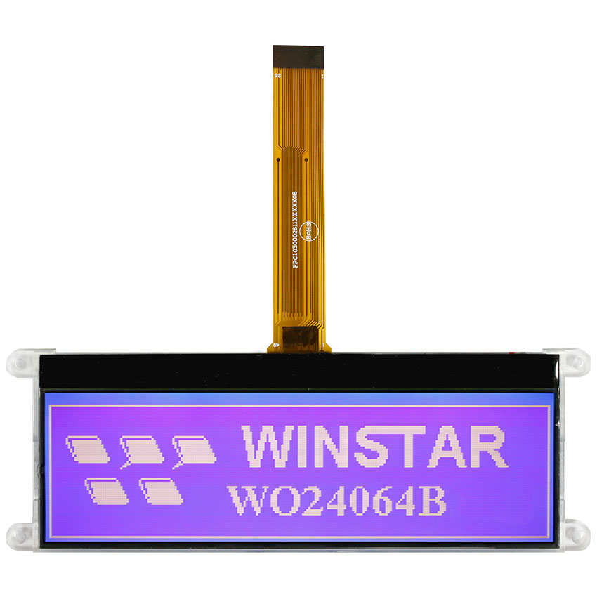
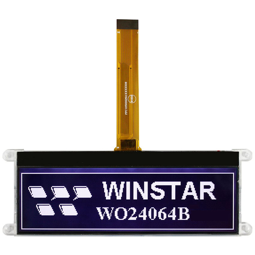
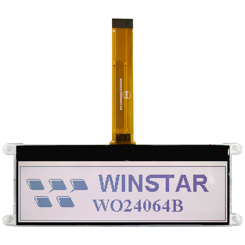
WO24064Bは、5.18インチ 240x64ドット モノクロCOG LCDモジュールです。ST7586SコントローラICを搭載し、6800、8080、3-Line SPI、4-Line SPIインターフェースに対応しています。ロジック電源は3.3Vです。
モジュールサイズは142.5 x 51.7 x 6.1 mm、表示エリア(VA)は129.0 x 37.6 mm、有効表示エリア(AA)は127.7 x 33.89 mmです。LEDバックライトを搭載し、筐体への固定に便利な4か所の取付穴を備えています。LCDタイプおよびLEDバックライトの組み合わせはご要望に応じて選択可能です。カスタマイズをご希望の場合は、上部のお問い合わせに追加よりご要望をご記入ください。
WO24064Bは、WO24064シリーズの中で最も大きな外形サイズを採用したモデルで、産業機器、計測機器、医療機器、自動化システム、各種組込みHMI機器に適しています。
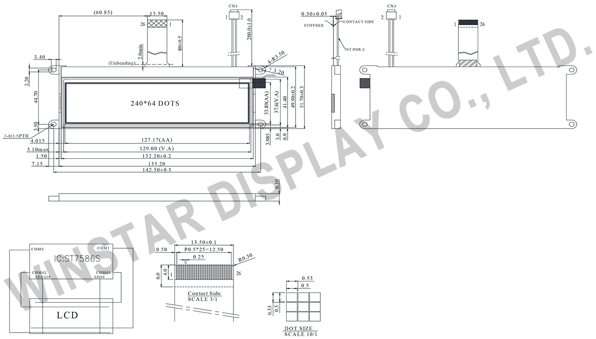
| 項目 | 標準値 | 単位 |
|---|---|---|
| 表示ドット数 | 240 x 64 | - |
| モジュールサイズ | 142.5 x 51.7 x 6.1 | mm |
| 表示エリア | 129.0 x 37.6 | mm |
| 有効エリア | 127.7 x 33.89 | mm |
| ドットサイズ | 0.5 x 0.5 | mm |
| ドットピッチ | 0.53 x 0.53 | mm |
| 駆動方法 | 1/64 | |
| バックライトタイプ | LED | |
| IC | ST7586S-G4 | |
| インターフェイス | 6800/8080/3-Line/4-Line | |
| 項目 | 記号 | 最小値 | 典型値 | 最大値 | 単位 |
|---|---|---|---|---|---|
| 操作温度 | TOP | -20 | - | +70 | ℃ |
| 保存温度 | TST | -30 | - | +80 | ℃ |
| デジタル電源電圧 | VDDI | -0.3 | - | 3.6 | V |
| アナログ電源電圧 | VDDA | -0.3 | - | 3.6 | V |
| LCD電源電圧 | V0-XV0 | -0.3 | - | 19 | V |
| LCD電源電圧 | VG | -0.3 | - | 5.5 | V |
| 項目 | 記号 | 条件 | 最小値 | 典型値 | 最大値 | 単位 |
|---|---|---|---|---|---|---|
| ロジック電源電圧 | VDD-VSS | - | 3.0 | 3.3 | 3.4 | V |
| LCM供給電圧 | V0-XV0 | Ta=-20℃ Ta=25℃ Ta=70℃ |
- 9.8 - |
- 10.0 - |
- 10.2 - |
V V V |
| 高レベル入力電圧 | VIH | - | 0.7 VDD | - | VDD | V |
| 低レベル入力電圧 | VIL | - | VSS | - | 0.3VDD | V |
| 高レベル出力電圧 | VOH | - | 0.8VDD | - | VDD | V |
| 低レベル出力電圧 | VOL | - | VSS | - | 0.2VDD | V |
| 供給電流 | IDD | VDD=3.3V | - | 1.5 | - | mA |
| Pin No. | 記号 | Level | 説明 | ||||||||||||||||||||
|---|---|---|---|---|---|---|---|---|---|---|---|---|---|---|---|---|---|---|---|---|---|---|---|
| 1 | VG | P | VG is the power of SEG-drivers. | ||||||||||||||||||||
| 2 | XV0 | P | Negative operating voltage of COM-drivers. | ||||||||||||||||||||
| 3 | V0 | P | Positive operating voltage of COM-drivers. V0O is the output of the positive Vop generator. V0I is the positive Vop supply of LCD drivers. V0S is the sensor of the positive Vop generator. V0O, V0I & V0S should be separated on ITO and be connected together by FPC. |
||||||||||||||||||||
| 4 | VM | P | VM is the non-select voltage level of COM-drivers. | ||||||||||||||||||||
| 5 | VDDA | P | Analog power for internal booster. | ||||||||||||||||||||
| 6 | VSS | P | Ground | ||||||||||||||||||||
| 7 | VD1 | P | VD1I is the power source of digital circuits. | ||||||||||||||||||||
| 8 | VDDI | P | Power of interface I/O circuit. | ||||||||||||||||||||
| 9 | CSB | Input | Chip select input pin. CSB=“L”: This chip is selected and the MPU interface is active. CSB=“H”: This chip is not selected and the MPU interface is disabled (D[7:0] are high impedance). |
||||||||||||||||||||
| 10 | IF3 | Input | These pins select interface operation mode.
|
||||||||||||||||||||
| 11 | IF2 | ||||||||||||||||||||||
| 12 | IF1 | ||||||||||||||||||||||
| 13 | RSTB | Input | Reset input pin. When RSTB is “L”, internal initialization procedure is executed. | ||||||||||||||||||||
| 14 | /RD(E) | Input | Read / Write execution control pin. (This pin is only used in parallel interface) | ||||||||||||||||||||
| 15 | D7 | I/O | The bi-directional data bus of the MPU interface. When CSB is “H”, they are high impedance. If using serial interface: D0 is the SDA signal in 4-Line & 3-Line interface. D1 is the A0 signal in 4-Line interface |
||||||||||||||||||||
| 16 | D6 | ||||||||||||||||||||||
| 17 | D5 | ||||||||||||||||||||||
| 18 | D4 | ||||||||||||||||||||||
| 19 | D3 | ||||||||||||||||||||||
| 20 | D2 | ||||||||||||||||||||||
| 21 | D1 | ||||||||||||||||||||||
| 22 | D0 | ||||||||||||||||||||||
| 23 | NC | No connection | |||||||||||||||||||||
| 24 | /WR(R/W) | Input | Read / Write execution control pin. (This pin is only used in parallel interface) | ||||||||||||||||||||
| 25 | A0(SCL) | Input | The function of this pin is different in parallel and serial interface. In parallel interface: A0 is register selection input. A0 = "H": inputs on data bus are display data; A0 = "L": inputs on data bus are command. _ In serial interface: this pad will be used as SCL (serial-clock) input |
||||||||||||||||||||
| 26 | VSS | P | Ground |


「すべてのクッキーを許可」をクリックすると、サイトのナビゲーションを向上させ、サイト使用状況を分析し、マーケティングおよびパフォーマンスの取り組みを支援するために、クッキーをデバイスに保存することに同意したことになります。この件に関する詳細情報は、ポリシーをご覧ください。プライバシーポリシー