 - WF24LSYAJDNG0")

我們重視您的隱私
通過點擊「允許所有 Cookie」,代表您同意在您的設備上存儲 Cookie 以增強網站瀏覽體驗、分析網站使用情況並協助我們的行銷和網站效能優化工作。您可以在我們的隱私權政策中找到有關於此的更多資訊。

 - WF24LSYAJDNN0")
 - WF24LSYAJDNN0")
 - WF24LSYAJDNN0")
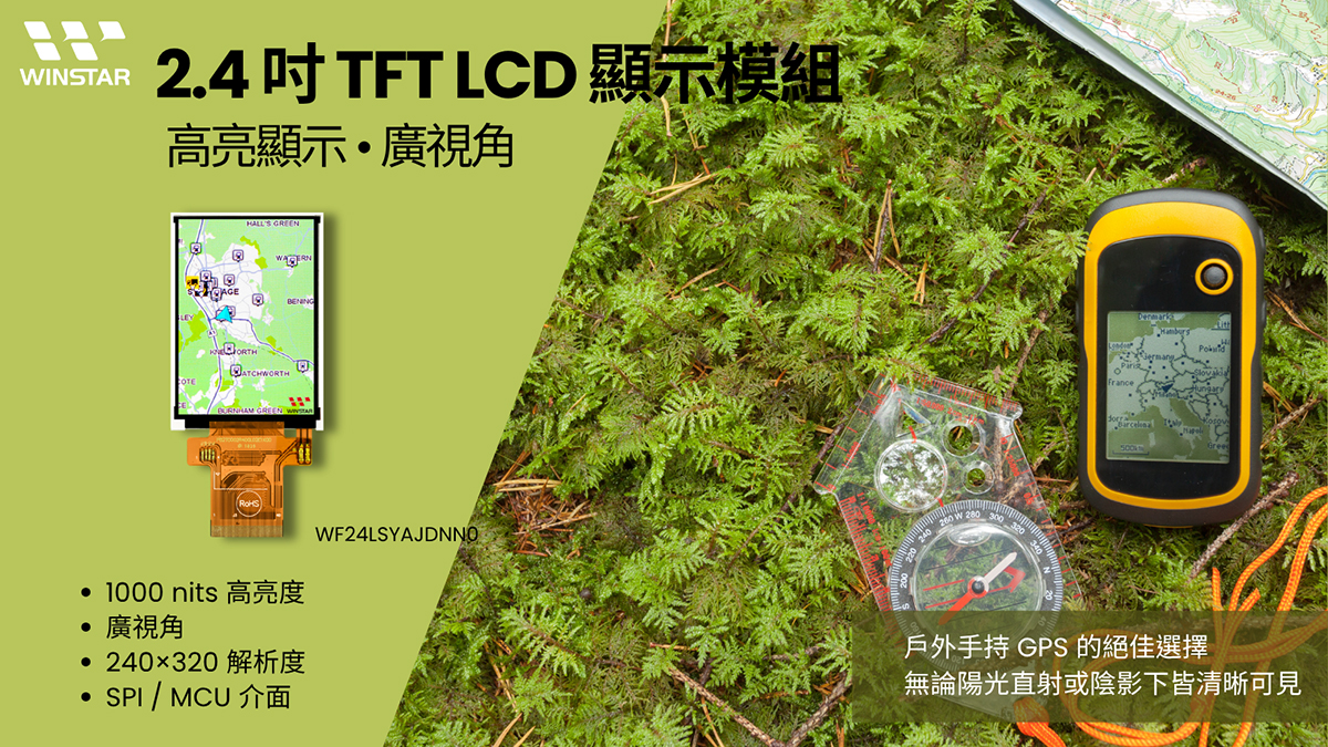
WF24LSYAJDNN0 是一款 2.4 吋直式 IPS TFT 顯示模組,解析度為 240x320 像素,具備 1000 nits 的高亮度,即使在強光環境下也能提供優異的可讀性。其四個方向為 80度廣視角與 800:1 對比度,可呈現鮮明且穩定的影像品質,適用於垂直方向的應用範圍。
WF24LSYAJDNN0 模組採用廣泛應用的 ILI9341V 驅動 IC,支援 80 MCU 8/16/9-bit 並列介面與 3-wire 9-bit / 4-wire 8-bit SPI 序列介面。LED 背光壽命超過 30,000 小時,搭配寬溫設計,特別適用於手持裝置、醫療儀器及戶外控制面板等對直式顯示有需求的設備。
| 項目 | 規格 | 單位 |
|---|---|---|
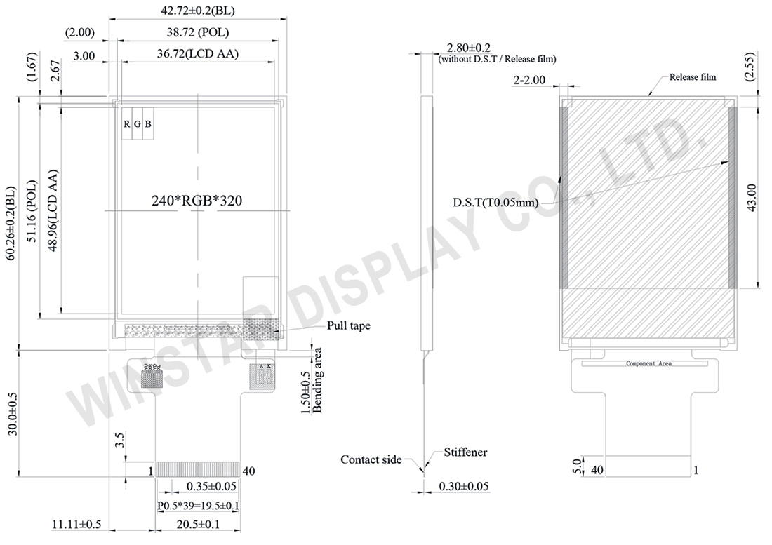
| 尺寸 (對角線) | 2.4 | 吋 |
| 解析度 | 240 × RGB × 320(TFT) | dots |
| 模組尺寸 | 42.72(W) × 60.26(H) × 2.8(D) | mm |
| 有效區域 | 36.72 × 48.96 | mm |
| 像素間距 | 0.153 × 0.153 | mm |
| LCD類型 | TFT全透 | |
| 控制器IC | ILI9341V 或相容IC | |
| 視角 | 80/80/80/80 | |
| 長寬比 | 直屏 | |
| 背光類型 | LED ,平常白 | |
| 觸控面板 | 無觸控面板 | |
| 表面 | 亮面 | |
| 項目 | 符號 | 最小值 | 典型值 | 最大值 | 單位 |
|---|---|---|---|---|---|
| 工作溫度 | TOP | -20 | - | +70 | ℃ |
| 儲存溫度 | TST | -30 | - | +80 | ℃ |
| 項目 | 符號 | 最小值 | 典型值 | 最大值 | 單位 |
|---|---|---|---|---|---|
| 類比電源電壓 | VCI | 2.5 | — | 3.3 | V |
| 邏輯電源電壓 | IOVCC | 2.5 | — | 3.3 | V |
| LCM電源電壓 | ICC | — | 6 | 9 | mA |
| 參數 | 符號 | 最小值 | 典型值 | 最大值 | 單位 |
|---|---|---|---|---|---|
| LED電流 | — | — | 40 | — | mA |
| LED電壓 | VBL+ | 10.8 | 11.6 | 12.4 | V |
| LED使用壽命 | — | 30,000 | — | — | Hr |
| NO | 符號 | 功能 | I/O | ||||||||||||||||||||||||||||||||||||||||||||
|---|---|---|---|---|---|---|---|---|---|---|---|---|---|---|---|---|---|---|---|---|---|---|---|---|---|---|---|---|---|---|---|---|---|---|---|---|---|---|---|---|---|---|---|---|---|---|---|
| 1 | GND | Ground | P | ||||||||||||||||||||||||||||||||||||||||||||
| 2-6 | NC | No connection | - | ||||||||||||||||||||||||||||||||||||||||||||
| 7 | VCI | High voltage power supply for analog circuit blocks (2.5 ~ 3.3 V) |
P | ||||||||||||||||||||||||||||||||||||||||||||
| 8 | IOVCC | Low voltage power supply for interface logic circuits (2.5 ~ 3.3 V) |
P | ||||||||||||||||||||||||||||||||||||||||||||
| 9 | TE | Tearing effect output pin to synchronize MPU to frame writing, activated by S/W command. When this pin is not activated, this pin is low. If not used, open this pin. |
O | ||||||||||||||||||||||||||||||||||||||||||||
| 10 | CS | Chip select signal. | I | ||||||||||||||||||||||||||||||||||||||||||||
| 11 | D/CX(SCL) | (D/CX): This pin is used to select “Data or Command” in the parallel interface. When DCX = 1, data is selected. When DCX = 0, command is selected. (SCL): This pin is used as the serial interface clock in 3-wire 9-bit/4-wire 8-bit serial data interface. If not used, this pin should be connected to IOVCC or GND. |
I | ||||||||||||||||||||||||||||||||||||||||||||
| 12 | WR(SPI_D/C) | (WRX) - 8080-Ⅰ/8080-Ⅱ system: Serves as a write signal and writes data at the rising edge. (D/CX) - 4-line system: Serves as the selector of command or parameter. Fix to IOVCC level when not in use. |
I | ||||||||||||||||||||||||||||||||||||||||||||
| 13 | RD | 8080-Ⅰ/8080-Ⅱ system (RDX): Serves as a read signal and MCU read data at the rising edge. Fix to IOVCC level when not in use. |
I | ||||||||||||||||||||||||||||||||||||||||||||
| 14-29 | DB0~DB15 | 18-bit parallel bi-directional data bus for MCU system. Fix to GND level when not in use. |
I/O | ||||||||||||||||||||||||||||||||||||||||||||
| 30 | RESET | This signal will reset the device and must be applied to properly initialize the chip. Signal is active low. |
I | ||||||||||||||||||||||||||||||||||||||||||||
| 31 | IM0 | Select the MCU interface mode
If use RGB Interface must select serial interface. * : Fix this pin at IOVCC or GND. |
I | ||||||||||||||||||||||||||||||||||||||||||||
| 32 | IM1 | ||||||||||||||||||||||||||||||||||||||||||||||
| 33 | IM2 | ||||||||||||||||||||||||||||||||||||||||||||||
| 34 | DB16 | 18-bit parallel bi-directional data bus for MCU system and RGB interface mode Fix to GND level when not in use. |
I/O | ||||||||||||||||||||||||||||||||||||||||||||
| 35 | DB17 | ||||||||||||||||||||||||||||||||||||||||||||||
| 36 | VLED- | Cathode of LED backlight. | P | ||||||||||||||||||||||||||||||||||||||||||||
| 37 | VLED- | Cathode of LED backlight. | P | ||||||||||||||||||||||||||||||||||||||||||||
| 38 | VLED+ | Anode of LED backlight. | P | ||||||||||||||||||||||||||||||||||||||||||||
| 39 | SDA | SDA : Serial in/out signal. The data is applied on the rising edge of the SCL signal. If not used, fix this pin at IOVCC or GND. |
I/O | ||||||||||||||||||||||||||||||||||||||||||||
| 40 | NC | Not used, open this pin | N | ||||||||||||||||||||||||||||||||||||||||||||

通過點擊「允許所有 Cookie」,代表您同意在您的設備上存儲 Cookie 以增強網站瀏覽體驗、分析網站使用情況並協助我們的行銷和網站效能優化工作。您可以在我們的隱私權政策中找到有關於此的更多資訊。