 - WF24LSYAJDNG0")


我们重视您的隐私
通过点击「允许所有 Cookie」,代表您同意在您的设备上存储 Cookie 以增强网站浏览体验、分析网站使用情况并协助我们的营销和网站效能优化工作。您可以在我们的隐私权政策中找到有关于此的更多信息。
 - WF24LSYAJDNN0")
 - WF24LSYAJDNN0")
 - WF24LSYAJDNN0")
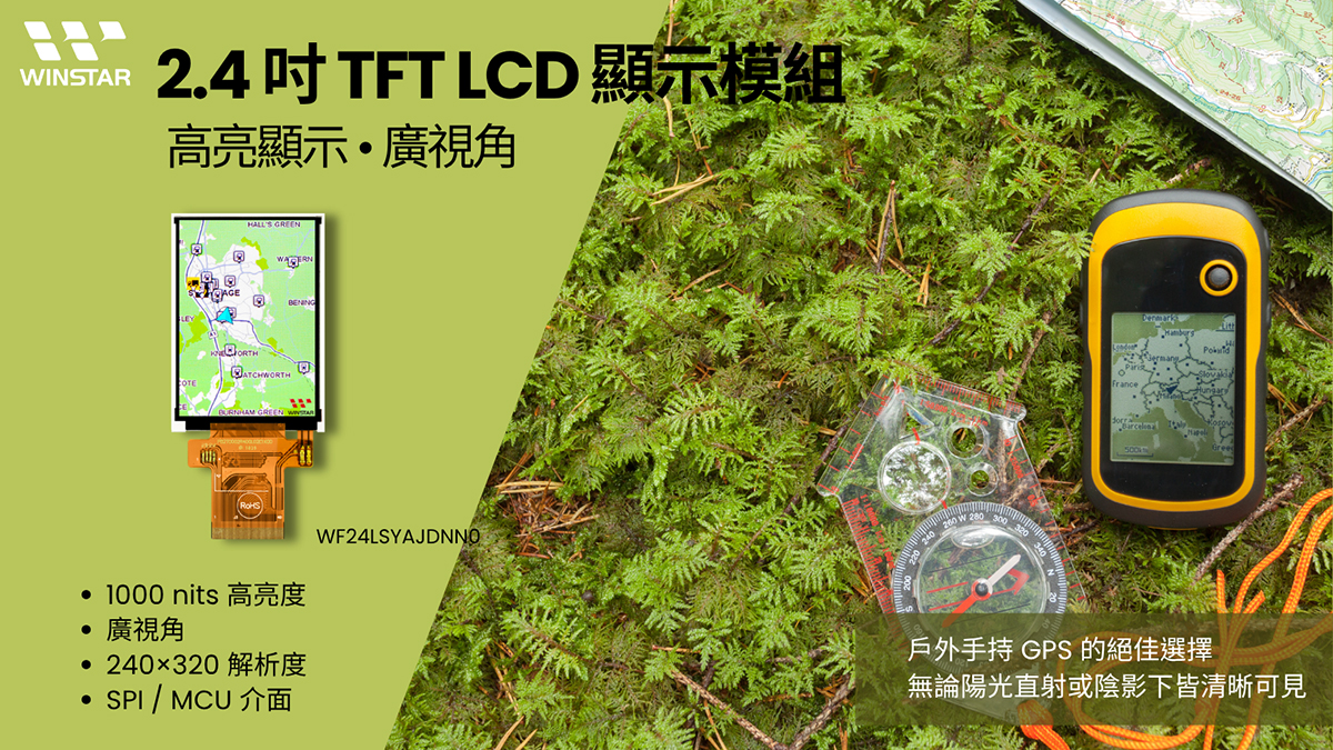
WF24LSYAJDNN0 是一款 2.4 英寸竖屏 IPS TFT 显示模块,分辨率为 240x320 像素,亮度高达 1000 nits,在强光环境下依然具备出色的可读性。该显示屏具备四个方向 80° 的宽视角和 800:1 的对比度,为紧凑型竖屏应用提供鲜艳且一致的图像品质。
WF24LSYAJDNN0 模块采用广泛应用的 ILI9341V 驱动 IC,支持 80 MCU 8/16/9-bit并行接口,以及 3 线 9-bit / 4 线 8-bit SPI 串行接口。具备宽工作温度范围与超过 30,000 小时的 LED 背光寿命,WF24LSYAJDNN0 非常适用于手持仪器、医疗设备和需要竖屏显示的户外控制面板等对显示性能有高要求的场景。
| 项目 | 规格 | 单位 |
|---|---|---|
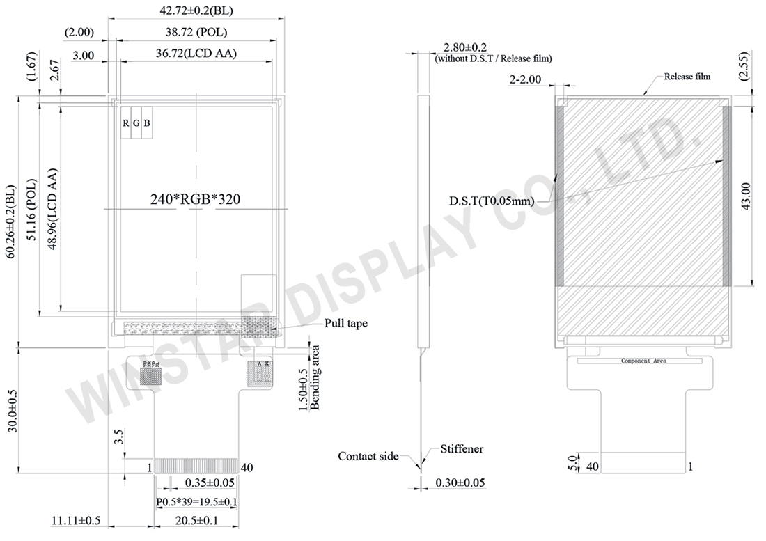
| 尺寸 (对角线) | 2.4 | 英寸 |
| 分辨率 | 240 × RGB × 320(TFT) | dots |
| 模块尺寸 | 42.72(W) × 60.26(H) × 2.8(D) | mm |
| 有效区域 | 36.72 × 48.96 | mm |
| 像素间距 | 0.153 × 0.153 | mm |
| LCD类型 | TFT全透 | |
| 控制器IC | ILI9341V 或相容IC | |
| 视角 | 80/80/80/80 | |
| 长宽比 | 直屏 | |
| 背光类型 | LED ,平常白 | |
| 触控面板 | 无触控面板 | |
| 表面 | 亮面 | |
| 项目 | 符号 | 最小值 | 典型值 | 最大值 | 单位 |
|---|---|---|---|---|---|
| 工作温度 | TOP | -20 | - | +70 | ℃ |
| 储存温度 | TST | -30 | - | +80 | ℃ |
| 参数 | 符号 | 最小值 | 典型值 | 最大值 | 单位 |
|---|---|---|---|---|---|
| 模拟电源电压 | VCI | 2.5 | — | 3.3 | V |
| 逻辑电源电压 | IOVCC | 2.5 | — | 3.3 | V |
| LCM电源电压 | ICC | — | 6 | 9 | mA |
| 参数 | 符号 | 最小值 | 典型值 | 最大值 | 单位 |
|---|---|---|---|---|---|
| LED电流 | — | — | 40 | — | mA |
| LED电压 | VBL+ | 10.8 | 11.6 | 12.4 | V |
| LED使用寿命 | — | 30,000 | — | — | Hr |
| NO | 符号 | 功能 | I/O | ||||||||||||||||||||||||||||||||||||||||||||
|---|---|---|---|---|---|---|---|---|---|---|---|---|---|---|---|---|---|---|---|---|---|---|---|---|---|---|---|---|---|---|---|---|---|---|---|---|---|---|---|---|---|---|---|---|---|---|---|
| 1 | GND | Ground | P | ||||||||||||||||||||||||||||||||||||||||||||
| 2-6 | NC | No connection | - | ||||||||||||||||||||||||||||||||||||||||||||
| 7 | VCI | High voltage power supply for analog circuit blocks (2.5 ~ 3.3 V) |
P | ||||||||||||||||||||||||||||||||||||||||||||
| 8 | IOVCC | Low voltage power supply for interface logic circuits (2.5 ~ 3.3 V) |
P | ||||||||||||||||||||||||||||||||||||||||||||
| 9 | TE | Tearing effect output pin to synchronize MPU to frame writing, activated by S/W command. When this pin is not activated, this pin is low. If not used, open this pin. |
O | ||||||||||||||||||||||||||||||||||||||||||||
| 10 | CS | Chip select signal. | I | ||||||||||||||||||||||||||||||||||||||||||||
| 11 | D/CX(SCL) | (D/CX): This pin is used to select “Data or Command” in the parallel interface. When DCX = 1, data is selected. When DCX = 0, command is selected. (SCL): This pin is used as the serial interface clock in 3-wire 9-bit/4-wire 8-bit serial data interface. If not used, this pin should be connected to IOVCC or GND. |
I | ||||||||||||||||||||||||||||||||||||||||||||
| 12 | WR(SPI_D/C) | (WRX) - 8080-Ⅰ/8080-Ⅱ system: Serves as a write signal and writes data at the rising edge. (D/CX) - 4-line system: Serves as the selector of command or parameter. Fix to IOVCC level when not in use. |
I | ||||||||||||||||||||||||||||||||||||||||||||
| 13 | RD | 8080-Ⅰ/8080-Ⅱ system (RDX): Serves as a read signal and MCU read data at the rising edge. Fix to IOVCC level when not in use. |
I | ||||||||||||||||||||||||||||||||||||||||||||
| 14-29 | DB0~DB15 | 18-bit parallel bi-directional data bus for MCU system. Fix to GND level when not in use. |
I/O | ||||||||||||||||||||||||||||||||||||||||||||
| 30 | RESET | This signal will reset the device and must be applied to properly initialize the chip. Signal is active low. |
I | ||||||||||||||||||||||||||||||||||||||||||||
| 31 | IM0 | Select the MCU interface mode
If use RGB Interface must select serial interface. * : Fix this pin at IOVCC or GND. |
I | ||||||||||||||||||||||||||||||||||||||||||||
| 32 | IM1 | ||||||||||||||||||||||||||||||||||||||||||||||
| 33 | IM2 | ||||||||||||||||||||||||||||||||||||||||||||||
| 34 | DB16 | 18-bit parallel bi-directional data bus for MCU system and RGB interface mode Fix to GND level when not in use. |
I/O | ||||||||||||||||||||||||||||||||||||||||||||
| 35 | DB17 | ||||||||||||||||||||||||||||||||||||||||||||||
| 36 | VLED- | Cathode of LED backlight. | P | ||||||||||||||||||||||||||||||||||||||||||||
| 37 | VLED- | Cathode of LED backlight. | P | ||||||||||||||||||||||||||||||||||||||||||||
| 38 | VLED+ | Anode of LED backlight. | P | ||||||||||||||||||||||||||||||||||||||||||||
| 39 | SDA | SDA : Serial in/out signal. The data is applied on the rising edge of the SCL signal. If not used, fix this pin at IOVCC or GND. |
I/O | ||||||||||||||||||||||||||||||||||||||||||||
| 40 | NC | Not used, open this pin | N | ||||||||||||||||||||||||||||||||||||||||||||

通过点击「允许所有 Cookie」,代表您同意在您的设备上存储 Cookie 以增强网站浏览体验、分析网站使用情况并协助我们的营销和网站效能优化工作。您可以在我们的隐私权政策中找到有关于此的更多信息。