


我們重視您的隱私
通過點擊「允許所有 Cookie」,代表您同意在您的設備上存儲 Cookie 以增強網站瀏覽體驗、分析網站使用情況並協助我們的行銷和網站效能優化工作。您可以在我們的隱私權政策中找到有關於此的更多資訊。


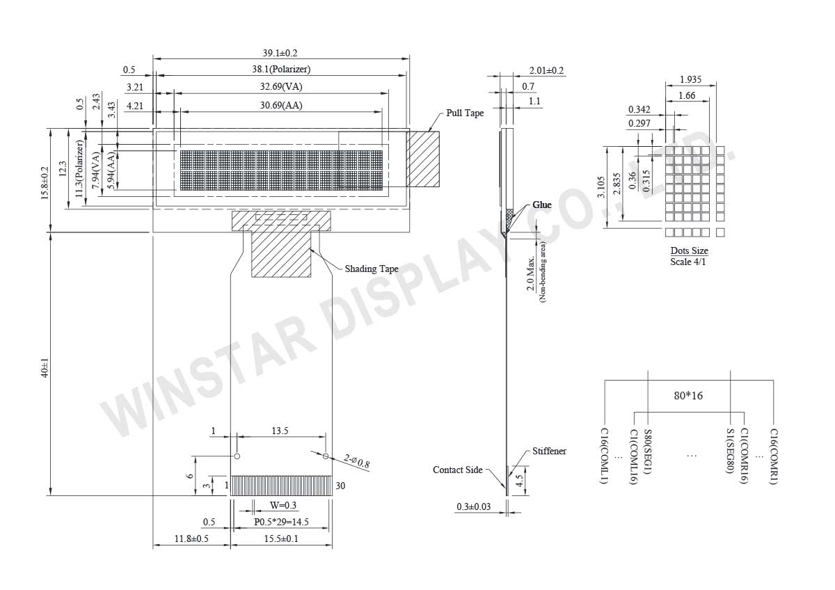
型號 WEO001602H
►類型: 字元
►結構: COG
►16字x2行
►IC:WS0012
►3.3V電源電壓
►1/16 duty
►介面: 6800, 8080, SPI, I2C
►發光顏色: 白色 / 黃色
WEO001602H是16x2字元型COG液晶模組。此模組內建WS0012控制器IC可支援I2C、4線SPI、6800和8080並列介面。邏輯電源電壓值為3.3V (VDD),顯示器電源電壓典型值為8.5V(VCC),50%顯示畫面耗電流為2mA @ VCC 8.5V (白色),驅動方式為1/16 duty。WEO001602H模組工作溫度為-40℃至+ 80℃,儲存溫度為-40℃至+85℃。
這款低功耗的16x2字元型OLED十分適合用來升級現有的 STN 字元顯示器。以下是這款 OLED 顯示器的優點。
►超快反應速度 — +25 ℃ -只需 10 μsec
►超廣視角 — 可達+/-175度
►輕薄 — 無需背光,自發光
►超高亮度
►高對比 — 10,000:1
►超廣溫
►低耗電流
| 項目 | 尺寸 | 單位 |
|---|---|---|
| 字元數 | 16 字 x 2行 | - |
| 模組尺寸 | 39.1 x 15.8 x 2.01 | mm |
| 檢視區域 | 32.69 x 7.94 | mm |
| 有效區域 | 30.69 x 5.94 | mm |
| 點大小 | 0.297 x 0.315 | mm |
| 點間距 | 0.342 x 0.36 | mm |
| 字元尺寸 | 1.66 x 2.835 | mm |
| 字元間距 | 1.935 x 3.105 | mm |
| 面板類型 | OLED , 單色 | |
| Duty | 1/16 | |
| IC | WS0012 | |
| 介面 | 6800, 8080, SPI, I2C | |
| 尺寸 | 1.23 吋 | |
| 項目 | 符號 | 最小值 | 最大值 | 單位 |
|---|---|---|---|---|
| 工作溫度 | TOP | -40 | +80 | °C |
| 儲存溫度 | TST | -40 | +85 | °C |
| 邏輯電源電壓 | VCC | -0.3 | 3.6 | V |
| DCDC轉換器電源電壓 | VCI | -0.3 | 3.6 | V |
| 顯示器電源電壓 | V16 | -0.3 | 19.0 | V |
| 項目 | 符號 | 條件 | 最小值 | 典型值 | 最大值 | 單位 |
|---|---|---|---|---|---|---|
| 邏輯電源電壓 | VCC | - | 2.6 | 3.3 | 3.5 | V |
| DCDC轉換器電源電壓 | VCI | - | 2.6 | 3.3 | 3.5 | V |
| 顯示器電源電壓 | V16 | - | - | 12.5 | 13.0 | V |
| 輸入高電壓 | VIH | - | 0.9xVCC | - | VCC | V |
| 輸入低電壓 | VIL | - | GND | - | 0.1xVCC | V |
| 輸出高電壓 | VOH | IOH=-0.5mA | 0.8xVCC | - | VCC | V |
| 輸出低電壓 | VOL | IOL=0.5mA | GND | - | 0.2xVCC | V |
| 50%顯示畫面耗電流 | I16 | V16=12.5V | - | 2 | 4 | mA |
| Pin No. | 符號 | Pin 類型 | 說明 | |||||||||||||||
|---|---|---|---|---|---|---|---|---|---|---|---|---|---|---|---|---|---|---|
| 1 | GND | P | Ground Pin | |||||||||||||||
| 2 | V16 | I | This is the most positive voltage supply pin of the chip. It can be supplied externally or generated internally by using internal DC-DC voltage converter. | |||||||||||||||
| 3 | VCI | P | DCDC buffer Power Supply | |||||||||||||||
| 4 | GND | P | Ground Pin | |||||||||||||||
| 5 | VCC | P | Power Pin | |||||||||||||||
| 6 | BVR | I | Brightness control pin. It should be connected to VCC. | |||||||||||||||
| 7 | DVR | I | Pre charge time control. It should be connected to VCC. | |||||||||||||||
| 8 | VBREF | O | This pin is the internal voltage reference of DCDC1 circuit. A stabilization capacitor should be connected between this pin and GND | |||||||||||||||
| 9 | RESE | I | NMOS source input pin: This pin connects to the source current pin of the external NMOS of the booster circuit. |
|||||||||||||||
| 10 | GDR | O | Gate drive pulse output pin: This output pin drives the gate of external NMOS of the booster circuit. |
|||||||||||||||
| 11 | FB | I | Feedback voltage input pin: This pin is the feedback resistor input of the booster circuit. It is used to adjust the booster output voltage level. |
|||||||||||||||
| 12 | VDD | P | Power Pin (connect to stabilization capacitor) | |||||||||||||||
| 13 | IM1 | I | Interface selection
|
|||||||||||||||
| 14 | IM0 | I | ||||||||||||||||
| 15 | RESETB | I | Reset pin | |||||||||||||||
| 16 | RS | I | Register Select Input Pin When this pin is set to "0", it is used as an Instruction Register. When this pin is set to "1", it is used for as the Data Register. |
|||||||||||||||
| 17 | CSB | I | Chip select input pins Data / instruction I/O is enabled only when CSB is “L”. |
|||||||||||||||
| 18 | RDB | I | Read / Write execution control pin
|
|||||||||||||||
| 19 | WRB | I | Read / Write execution control pin
|
|||||||||||||||
| 20 | SDA | I/O | SDA is the serial data input for I2C. | |||||||||||||||
| 21 | SDC | I/O | SDC is the serial clock input/output for I2C. | |||||||||||||||
| 22~25 | DB7~DB4 | I/O | High Order Bidirectional Data I/O Pins These pins are used for data transfer and reception between the MPU and WS0012. When SPI is selected, DB5 will be the serial clock input: SCL DB7 will be the serial data input: SDI. DB6 will be the serial data output: SDO. |
|||||||||||||||
| 26~29 | DB3~DB0 | I/O | Low Order Bidirectional Data I/O Pins These pins are used for data transfer and reception between the MPU and WS0012. These pins are not used during a 4-bit operation. |
|||||||||||||||
| 30 | GND | P | Ground Pin |

通過點擊「允許所有 Cookie」,代表您同意在您的設備上存儲 Cookie 以增強網站瀏覽體驗、分析網站使用情況並協助我們的行銷和網站效能優化工作。您可以在我們的隱私權政策中找到有關於此的更多資訊。