우리는 귀하의 프라이버시를 소중히 여깁니다
"모든 쿠키 허용"을 클릭하면 사이트 탐색을 개선하고, 사이트 사용을 분석하며, 마케팅 및 성능 노력에 도움을 주기 위해 쿠키를 귀하의 장치에 저장하는 데 동의한 것으로 간주됩니다. 이 주제에 대한 추가 정보는 당사의 정책에서 확인할 수 있습니다. 개인정보 보호정책


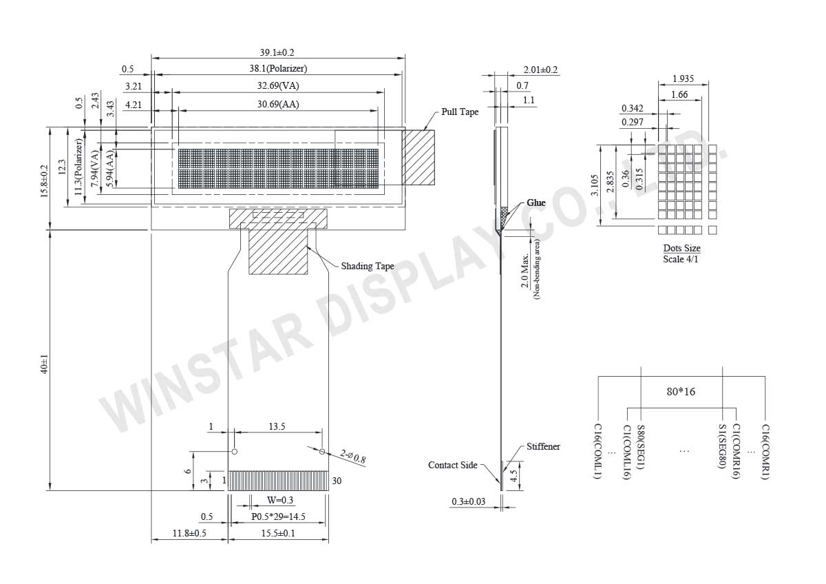
| 항목 | 치수 | 단위 |
|---|---|---|
| 디스플레이 형식 | 16 문자 x 2 라인 | - |
| 모듈 치수 | 39.1 x 15.8 x 2.01 | mm |
| 보기 영역 | 32.69 x 7.94 | mm |
| 활성 영역 | 30.69 x 5.94 | mm |
| 도트 크기 | 0.297 x 0.315 | mm |
| 도트 피치 | 0.342 x 0.36 | mm |
| 캐릭터 크기 | 1.66 x 2.835 | mm |
| 캐릭터 피치 | 1.935 x 3.105 | mm |
| Panel type | OLED , Monochrome | |
| Duty | 1/16 | |
| IC | WS0012 | |
| 인터페이스 | 6800, 8080, SPI, I2C | |
| 크기 | 1.23 인치 | |
| 항목 | 기호 | 최소값 | 최대값 | 단위 |
|---|---|---|---|---|
| 작동 온도 | TOP | -40 | +80 | °C |
| 보관 온도 | TST | -40 | +85 | °C |
| Supply Voltage For Logic | VCC | -0.3 | 3.6 | V |
| Supply Voltage For DCDC converter | VCI | -0.3 | 3.6 | V |
| Supply Voltage for Display | V16 | -0.3 | 19.0 | V |
| 항목 | 기호 | 조건 | 최소값 | 대표값 | 최대값 | 단위 |
|---|---|---|---|---|---|---|
| Supply Voltage For Logic | VCC | - | 2.6 | 3.3 | 3.5 | V |
| Supply Voltage For DCDC converter | VCI | - | 2.6 | 3.3 | 3.5 | V |
| Supply Voltage for Display | V16 | - | - | 12.5 | 13.0 | V |
| Input High Volt. | VIH | - | 0.9xVCC | - | VCC | V |
| Input Low Volt. | VIL | - | GND | - | 0.1xVCC | V |
| Output High Volt. | VOH | IOH=-0.5mA | 0.8xVCC | - | VCC | V |
| Output Low Volt. | VOL | IOL=0.5mA | GND | - | 0.2xVCC | V |
| 50% Checkerboard Operating Current |
I16 | V16=12.5V | - | 2 | 4 | mA |
| Pin No. | 기호 | Pin Type | 기능 | |||||||||||||||
|---|---|---|---|---|---|---|---|---|---|---|---|---|---|---|---|---|---|---|
| 1 | GND | P | Ground Pin | |||||||||||||||
| 2 | V16 | I | This is the most positive voltage supply pin of the chip. It can be supplied externally or generated internally by using internal DC-DC voltage converter. | |||||||||||||||
| 3 | VCI | P | DCDC buffer Power Supply | |||||||||||||||
| 4 | GND | P | Ground Pin | |||||||||||||||
| 5 | VCC | P | Power Pin | |||||||||||||||
| 6 | BVR | I | Brightness control pin. It should be connected to VCC. | |||||||||||||||
| 7 | DVR | I | Pre charge time control. It should be connected to VCC. | |||||||||||||||
| 8 | VBREF | O | This pin is the internal voltage reference of DCDC1 circuit. A stabilization capacitor should be connected between this pin and GND | |||||||||||||||
| 9 | RESE | I | NMOS source input pin: This pin connects to the source current pin of the external NMOS of the booster circuit. |
|||||||||||||||
| 10 | GDR | O | Gate drive pulse output pin: This output pin drives the gate of external NMOS of the booster circuit. |
|||||||||||||||
| 11 | FB | I | Feedback voltage input pin: This pin is the feedback resistor input of the booster circuit. It is used to adjust the booster output voltage level. |
|||||||||||||||
| 12 | VDD | P | Power Pin (connect to stabilization capacitor) | |||||||||||||||
| 13 | IM1 | I | Interface selection
|
|||||||||||||||
| 14 | IM0 | I | ||||||||||||||||
| 15 | RESETB | I | Reset pin | |||||||||||||||
| 16 | RS | I | Register Select Input Pin When this pin is set to "0", it is used as an Instruction Register. When this pin is set to "1", it is used for as the Data Register. |
|||||||||||||||
| 17 | CSB | I | Chip select input pins Data / instruction I/O is enabled only when CSB is “L”. |
|||||||||||||||
| 18 | RDB | I | Read / Write execution control pin
|
|||||||||||||||
| 19 | WRB | I | Read / Write execution control pin
|
|||||||||||||||
| 20 | SDA | I/O | SDA is the serial data input for I2C. | |||||||||||||||
| 21 | SDC | I/O | SDC is the serial clock input/output for I2C. | |||||||||||||||
| 22~25 | DB7~DB4 | I/O | High Order Bidirectional Data I/O Pins These pins are used for data transfer and reception between the MPU and WS0012. When SPI is selected, DB5 will be the serial clock input: SCL DB7 will be the serial data input: SDI. DB6 will be the serial data output: SDO. |
|||||||||||||||
| 26~29 | DB3~DB0 | I/O | Low Order Bidirectional Data I/O Pins These pins are used for data transfer and reception between the MPU and WS0012. These pins are not used during a 4-bit operation. |
|||||||||||||||
| 30 | GND | P | Ground Pin |

"모든 쿠키 허용"을 클릭하면 사이트 탐색을 개선하고, 사이트 사용을 분석하며, 마케팅 및 성능 노력에 도움을 주기 위해 쿠키를 귀하의 장치에 저장하는 데 동의한 것으로 간주됩니다. 이 주제에 대한 추가 정보는 당사의 정책에서 확인할 수 있습니다. 개인정보 보호정책