 - WG12232J")
 - WG12232L")
我们重视您的隐私
通过点击「允许所有 Cookie」,代表您同意在您的设备上存储 Cookie 以增强网站浏览体验、分析网站使用情况并协助我们的营销和网站效能优化工作。您可以在我们的隐私权政策中找到有关于此的更多信息。


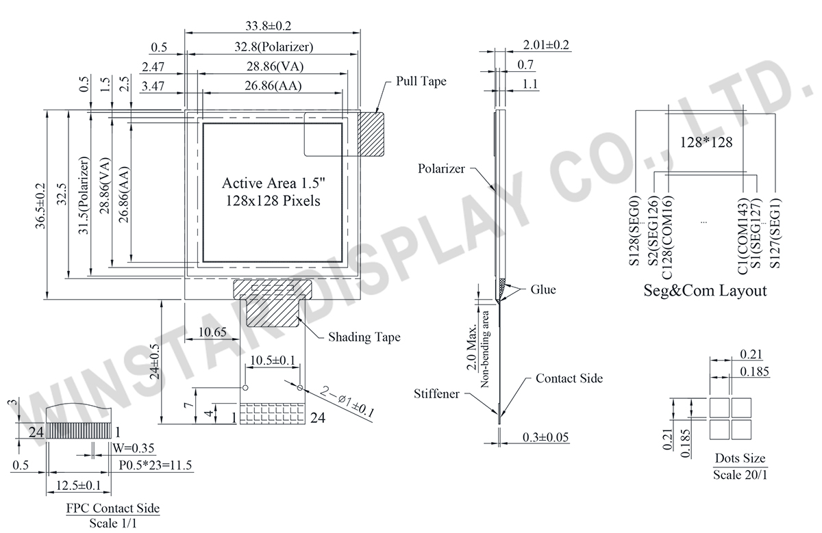
WEO128128H是一款1.5寸COG图形OLED显示器模块,显示画面由128x128像素组成,且支持4位灰阶功能。
此模块电源电压典型值为 3V,显示器电源电压典型值为12V,内建CH1120控制器IC,可支持I2C、SPI及8080并列接口;50%显示画面耗电流为20mA @ VCC 12V (白色)及14.5 V(黄色)。
WEO128128H COG OLED模块体积小、低功耗、轻薄,非常适合适用于智能家居应用、云/物联网系统、手持式仪器、智能技术设备、能源系统、汽车、通信系统、医疗仪器等。 WEO128128H 模块工作温度为-40℃至+ 80℃,储存温度为-40℃至+85℃。
| 项目 | 规格说明 | 单位 |
|---|---|---|
| 点阵(分辨率) | 128 × 128 | dots |
| 模块尺寸 | 33.80 x 36.50 x 2.01 | mm |
| 有效区域 | 26.86 x 26.86 | mm |
| 像素大小 | 0.185 x 0.185 | mm |
| 像素间距 | 0.210 x 0.210 | mm |
| 显示模式 | Passive Matrix | |
| 显示颜色 | Monochrome | |
| 驱动方式 | 1/128 Duty | |
| Gray Scale | 4 bits | |
| IC | CH1120 | |
| 接口 | 8080,SPI,I2C | |
| 尺寸 | 1.5 inch | |
| 参数 | 符号 | 最小值 | 最大值 | 单位 |
|---|---|---|---|---|
| 逻辑电源电压 | VDD | -0.3 | 3.5 | V |
| 显示电源电压 | VPP | -0.3 | 15.0 | V |
| 工作温度 | TOP | -40 | +80 | °C |
| 储存温度 | TSTG | -40 | +85 | °C |
| 项目 | 符号 | 条件 | 最小值 | 典型值 | 最大值 | 单位 |
|---|---|---|---|---|---|---|
| 逻辑电源电压 | VDD | - | 1.65 | 3.0 | 3.3 | V |
| 显示电源电压 | VPP | - | 8.0 | 14.5 | 15.0 | V |
| 输入高电压 | VIH | - | 0.8×VDD | - | VDD | V |
| 输入低电压 | VIL | - | GND | - | 0.2×VDD | V |
| 输出高电压 | VOH | - | 0.8×VDD | - | VDD | V |
| 输出低电压 | VOL | - | GND | - | 0.1×VDD | V |
| Display 50% Pixel on | IPP | VPP=14.5V | - | 20 | 30 | mA |
| No. | 符号 | 功能说明 | |||||||||||||||
|---|---|---|---|---|---|---|---|---|---|---|---|---|---|---|---|---|---|
| 1 | ESD_GND | This pin should be connected to GND. | |||||||||||||||
| 2 | VPP | This is the most positive voltage supply pin of the chip. It should be supplied externally. |
|||||||||||||||
| 3 | VCOMH | This is a pin for the voltage output high level for common signals. A capacitor should be connected between this pin and GND. |
|||||||||||||||
| 4 | VDD | Power supply for logic | |||||||||||||||
| 5 | NC | No connection | |||||||||||||||
| 6 | IM1 | These are the MPU interface mode select pins.
|
|||||||||||||||
| 7 | IM2 | ||||||||||||||||
| 8 | VSS | Ground for logic and analog. This pin should be connected to GND externally. | |||||||||||||||
| 9 | IREF | This is a segment current reference pin. A resistor should be connected between this pin and GND. |
|||||||||||||||
| 10 | CSB | This pin is the chip select input. When CSB = “L”, then the chip select becomes active, and data/command I/O is enabled. When in I2C interface, this pin is not used, so it must be connected to “L”. |
|||||||||||||||
| 11 | RESB | This is a reset signal input pin. When RESB is set to “L”, the settings are initialized. The reset operation is performed by the RESB signal level. This pin internal pull high. | |||||||||||||||
| 12 | A0 | This is the Data/Command control pin that determines whether the data bits are data or a command. A0 = “H”: the inputs at D0 to D7 are treated as display data A0 = “L”: the inputs at D0 to D7 are transferred to the command registers. In I2C interface, this pin serves as SA0 to distinguish the different address of OLED driver. When in 3-wire interface, this pin is not used, so it must be connected to “L”. |
|||||||||||||||
| 13 | WRB | This is a MPU interface input pin. When connected to an 8080 MPU, this is active LOW. This pin connects to the 8080 MPU WR signal. The signals on the data bus are latched at the rising edge of the WR signal When in 3-wire.4-wire & I2C interface, this pin is not used, so it must be connected to “L”. |
|||||||||||||||
| 14 | RDB | This is a MPU interface input pin. When connected to an 8080 series MPU, it is active LOW. This pin is connected to the RD signal of the 8080 series MPU, and the data bus is in an output status when this signal is “L”. When in 3-wire.4-wire & I2C interface, this pin is not used, so it must be connected to “L”. |
|||||||||||||||
| 15 | D0 | This is an 8-bit bi-directional data bus that connects to an 8-bit or 16-bit standard MPU data bus. When the serial interface(SPI) and I2C is selected, then D0 serves as the serial clock input pin (SCL) and D1 serves as the serial data input pin (SI). At this time, D2 to D7 are set to high impedance. D7~D2 is recommended to connect the VDD or GND. It is also allowed to leave D7~D2 unconnected. |
|||||||||||||||
| 16 | D1 | ||||||||||||||||
| 17 | D2 | ||||||||||||||||
| 18 | D3 | ||||||||||||||||
| 19 | D4 | ||||||||||||||||
| 20 | D5 | ||||||||||||||||
| 21 | D6 | ||||||||||||||||
| 22 | D7 | ||||||||||||||||
| 23 | VPP | This is the most positive voltage supply pin of the chip It should be supplied externally. |
|||||||||||||||
| 24 | ESD_GND | This pin should be connected to GND. |

通过点击「允许所有 Cookie」,代表您同意在您的设备上存储 Cookie 以增强网站浏览体验、分析网站使用情况并协助我们的营销和网站效能优化工作。您可以在我们的隐私权政策中找到有关于此的更多信息。