私たちはあなたのプライバシーを大切にします
「すべてのクッキーを許可」をクリックすると、サイトのナビゲーションを向上させ、サイト使用状況を分析し、マーケティングおよびパフォーマンスの取り組みを支援するために、クッキーをデバイスに保存することに同意したことになります。この件に関する詳細情報は、ポリシーをご覧ください。プライバシーポリシー


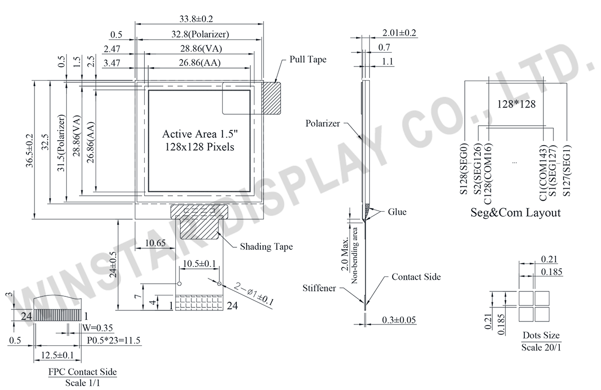
WEO128128H はグレースケール機能を備えた1.5 インチ COG グラフィック OLED ディスプレイです。解像度は 128x128ドットでCH1120 IC搭載で8080、SPI、I2C インターフェイス、1/128 駆動デューティをサポートいたします。ロジック電源電圧は 3V (VDD)でディスプレイ電源電圧は 12V です。そして、50% チェッカーボード表示での電流と言えば 20mA(白@ VCC 12V/黄@VCC 14.5V)です。
WEO128128Hはスマート ホーム アプリケーション、クラウド/IoT システム、ハンドヘルド機器、インテリジェント テクノロジー デバイス、エネルギー システム、交通関係、通信システム、医療機器などに適しております。その動作温度範囲は-40℃ ~ +80℃で、保管温度範囲は-40℃~+85℃です。
| 項目 | 仕様 | 単位 |
|---|---|---|
| ドットマトリックス(解像度) | 128 × 128 | dots |
| モジュールサイズ | 33.80 x 36.50 x 2.01 | mm |
| 有効エリア | 26.86 x 26.86 | mm |
| ドットサイズ | 0.185 x 0.185 | mm |
| ドットピッチ | 0.210 x 0.210 | mm |
| 表示モード | Passive Matrix | |
| 発光色 | Monochrome | |
| 駆動方法 | 1/128 Duty | |
| グレースケール | 4 bits | |
| IC | CH1120 | |
| インターフェイス | 8080,SPI,I2C | |
| 表示サイズ(対角線) | 1.5 inch | |
| パラメーター | 記号 | 最小値 | 最大值 | 単位 |
|---|---|---|---|---|
| ロジック電源電圧 | VDD | -0.3 | 3.5 | V |
| Display電源電圧 | VPP | -0.3 | 15.0 | V |
| 操作温度 | TOP | -40 | +80 | °C |
| 保存温度 | TSTG | -40 | +85 | °C |
| 項目 | 記号 | 条件 | 最小値 | 典型值 | 最大值 | 単位 |
|---|---|---|---|---|---|---|
| ロジック電源電圧 | VDD | - | 1.65 | 3.0 | 3.3 | V |
| Display電源電圧 | VPP | - | 8.0 | 14.5 | 15.0 | V |
| 高レベル入力電圧 | VIH | - | 0.8×VDD | - | VDD | V |
| 低レベル入力電圧 | VIL | - | GND | - | 0.2×VDD | V |
| 高レベル出力電圧 | VOH | - | 0.8×VDD | - | VDD | V |
| 低レベル出力電圧 | VOL | - | GND | - | 0.1×VDD | V |
| Display 50% Pixel on | IPP | VPP=14.5V | - | 20 | 30 | mA |
| No. | 記号 | 説明 | |||||||||||||||
|---|---|---|---|---|---|---|---|---|---|---|---|---|---|---|---|---|---|
| 1 | ESD_GND | This pin should be connected to GND. | |||||||||||||||
| 2 | VPP | This is the most positive voltage supply pin of the chip. It should be supplied externally. |
|||||||||||||||
| 3 | VCOMH | This is a pin for the voltage output high level for common signals. A capacitor should be connected between this pin and GND. |
|||||||||||||||
| 4 | VDD | Power supply for logic | |||||||||||||||
| 5 | NC | No connection | |||||||||||||||
| 6 | IM1 | These are the MPU interface mode select pins.
|
|||||||||||||||
| 7 | IM2 | ||||||||||||||||
| 8 | VSS | Ground for logic and analog. This pin should be connected to GND externally. | |||||||||||||||
| 9 | IREF | This is a segment current reference pin. A resistor should be connected between this pin and GND. |
|||||||||||||||
| 10 | CSB | This pin is the chip select input. When CSB = “L”, then the chip select becomes active, and data/command I/O is enabled. When in I2C interface, this pin is not used, so it must be connected to “L”. |
|||||||||||||||
| 11 | RESB | This is a reset signal input pin. When RESB is set to “L”, the settings are initialized. The reset operation is performed by the RESB signal level. This pin internal pull high. | |||||||||||||||
| 12 | A0 | This is the Data/Command control pin that determines whether the data bits are data or a command. A0 = “H”: the inputs at D0 to D7 are treated as display data A0 = “L”: the inputs at D0 to D7 are transferred to the command registers. In I2C interface, this pin serves as SA0 to distinguish the different address of OLED driver. When in 3-wire interface, this pin is not used, so it must be connected to “L”. |
|||||||||||||||
| 13 | WRB | This is a MPU interface input pin. When connected to an 8080 MPU, this is active LOW. This pin connects to the 8080 MPU WR signal. The signals on the data bus are latched at the rising edge of the WR signal When in 3-wire.4-wire & I2C interface, this pin is not used, so it must be connected to “L”. |
|||||||||||||||
| 14 | RDB | This is a MPU interface input pin. When connected to an 8080 series MPU, it is active LOW. This pin is connected to the RD signal of the 8080 series MPU, and the data bus is in an output status when this signal is “L”. When in 3-wire.4-wire & I2C interface, this pin is not used, so it must be connected to “L”. |
|||||||||||||||
| 15 | D0 | This is an 8-bit bi-directional data bus that connects to an 8-bit or 16-bit standard MPU data bus. When the serial interface(SPI) and I2C is selected, then D0 serves as the serial clock input pin (SCL) and D1 serves as the serial data input pin (SI). At this time, D2 to D7 are set to high impedance. D7~D2 is recommended to connect the VDD or GND. It is also allowed to leave D7~D2 unconnected. |
|||||||||||||||
| 16 | D1 | ||||||||||||||||
| 17 | D2 | ||||||||||||||||
| 18 | D3 | ||||||||||||||||
| 19 | D4 | ||||||||||||||||
| 20 | D5 | ||||||||||||||||
| 21 | D6 | ||||||||||||||||
| 22 | D7 | ||||||||||||||||
| 23 | VPP | This is the most positive voltage supply pin of the chip It should be supplied externally. |
|||||||||||||||
| 24 | ESD_GND | This pin should be connected to GND. |

「すべてのクッキーを許可」をクリックすると、サイトのナビゲーションを向上させ、サイト使用状況を分析し、マーケティングおよびパフォーマンスの取り組みを支援するために、クッキーをデバイスに保存することに同意したことになります。この件に関する詳細情報は、ポリシーをご覧ください。プライバシーポリシー