 - WEO025664D-CTP")
 - WEO025664D")
 - WF40ESWAA6MNN0")

我们重视您的隐私
通过点击「允许所有 Cookie」,代表您同意在您的设备上存储 Cookie 以增强网站浏览体验、分析网站使用情况并协助我们的营销和网站效能优化工作。您可以在我们的隐私权政策中找到有关于此的更多信息。
 - WEO025664E")
 - WEO025664E")
 - WEO025664E")
 - WEO025664E")
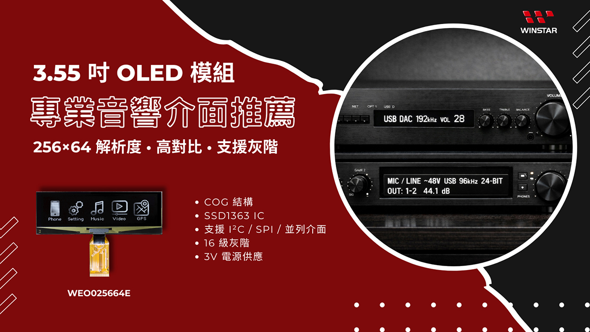
WEO025664E 是一款 3.55 寸 COG 结构的绘图型 OLED 显示屏,采用 256x64 点矩阵,并搭载 SSD1363 控制器 IC。此产品支持 4-bit(16 阶)灰阶显示,并提供多种接口选择:6800/8080 并列接口、3 线/4 线 SPI 接口及 I2C 接口。I2C 接口的加入,为设计需求简单通信与低功耗的应用提供了更多灵活性。
相比之下,WEO025664D 使用 SSD1322 控制器 IC,仅支持 6800/8080 并列及 SPI 接口,不支持 I2C。两款产品的显示分辨率与物理尺寸相同,但 WEO025664E 更适合需要多界面选择的应用。
两款产品均具有高对比度度、广视角以及 1/64 duty 驱动方案以达到高效能电源管理。WEO025664E 以 3.3V 逻辑电压与 16V 显示驱动电压运行,典型耗电为 35mA(50% 检查板图案,VCC=16V)。
WEO025664E 适用于长期稳定显示,应用于医疗设备、控制面板、自助结账系统,以及专业音频设备、Hi-Fi 系统和音频接口面板。工作温度范围 –40°C 至 +80°C,存储温度范围 –40°C 至 +85°C。
| 项目 | 规格 | 单位 |
|---|---|---|
| 点阵 | 256 x 64 Dots | - |
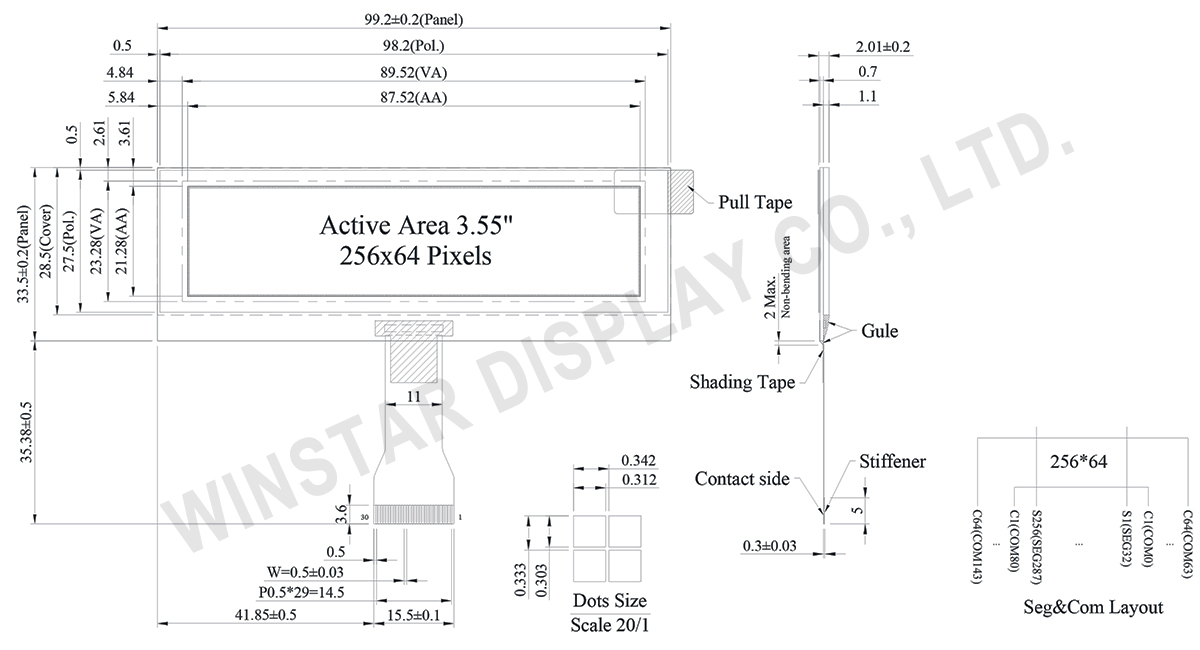
| 模块尺寸 | 99.2 × 33.5 × 2.01 | mm |
| 有效区域 | 87.52 × 21.28 | mm |
| 像素大小 | 0.312 × 0.303 | mm |
| 像素间距 | 0.342 × 0.333 | mm |
| 显示模式 | 被动矩阵 | |
| 显示颜色 | 单色 | |
| 驱动方式 | 1/64 Duty | |
| 灰阶 | 4 bits | |
| IC | SSD1363 | |
| 接口 | 6800,8080,4-Wire SPI,I2C | |
| 尺寸 | 3.55吋 | |
| 参数 | 符号 | 最小值 | 最大值 | 单位 |
|---|---|---|---|---|
| 供电电压 | VDD | -0.3 | 4.0 | V |
| 供电电压 | VCC | -0.5 | 19.0 | V |
| 工作温度 | TOP | -40 | 80 | °C |
| 储存温度 | TSTG | -40 | 85 | °C |
| 项目 | 符号 | 条件 | 最小值 | 典型值 | 最大值 | 单位 |
|---|---|---|---|---|---|---|
| 低压电源,输入 / 输出 Pin 电源 | VDD | - | 1.65 | 3.0 | 3.3 | V |
| 工作电压 | VCC | - | 8.0 | 16.0 | 16.5 | V |
| 输入高电压 | VIH | - | 0.8×VDD | - | VDD | V |
| 输入低电压 | VIL | - | 0 | - | 0.2×VDD | V |
| 输出高电压 | VOH | - | 0.9×VDD | - | VDD | V |
| 输出低电压 | VOL | - | 0 | - | 0.1×VDD | V |
| 显示屏 50% 像素开启 | ICC | VCC =16V | - | 30 | 45 | mA |
| Pin Number | 符号 | 功能说明 | |||||||||||||||
|---|---|---|---|---|---|---|---|---|---|---|---|---|---|---|---|---|---|
| 1 | ESD_GND | ESD Ground pin | |||||||||||||||
| 2 | VSS | Ground pin. It must be connected to external ground. | |||||||||||||||
| 3 | VCC | Power supply for panel driving voltage. This is also the most positive power voltage supply pin. A capacitor should be connected between this pin and VSS. |
|||||||||||||||
| 4 | VCOMH | COM signal deselected voltage level. A capacitor should be connected between this pin and VSS. |
|||||||||||||||
| 5 | VLSS | Analog system ground pin. It must be connected to external ground. | |||||||||||||||
| 6 | D7 | These pins are bi-directional data bus connecting to the MCU data bus. Unused pins are recommended to tie LOW. When serial interface mode is selected, D2, D1 should be tied together as the serial data input: SDIN, and D0 will be the serial clock input: SCLK. When I2C mode is selected, D2, D1 should be tied together and serve as SDAout, SDAin in application and D0 is the serial clock input, SCL. |
|||||||||||||||
| 7 | D6 | ||||||||||||||||
| 8 | D5 | ||||||||||||||||
| 9 | D4 | ||||||||||||||||
| 10 | D3 | ||||||||||||||||
| 11 | D2 | ||||||||||||||||
| 12 | D1 | ||||||||||||||||
| 13 | D0 | ||||||||||||||||
| 14 | E(RD#) | This pin is MCU interface input. When 6800 interface mode is selected, this pin will be used as the Enable (E) signal. Read/write operation is initiated when this pin is pulled HIGH and the chip is selected. When 8080 interface mode is selected, this pin receives the Read (RD#) signal. Read operation is initiated when this pin is pulled LOW and the chip is selected. When serial or I2C interface is selected, this pin must be connected to VSS. |
|||||||||||||||
| 15 | R/W# (WR#) | This pin is read / write control input pin connecting to the MCU interface. When 6800 interface mode is selected, this pin will be used as Read/Write (R/W#) selection input. Read mode will be carried out when this pin is pulled HIGH and write mode when LOW. When 8080 interface mode is selected, this pin will be the Write (WR#) input. Data write operation is initiated when this pin is pulled LOW and the chip is selected. When serial or I2C interface is selected, this pin must be connected to VSS. |
|||||||||||||||
| 16 | BS1 | MCU bus interface selection pins. Select appropriate logic setting as described in the following table. BS2 and BS1 are pin select.
(1) 0 is connected to VSS (2) 1 is connected to VDD |
|||||||||||||||
| 17 | BS2 | ||||||||||||||||
18 |
D/C# | This pin is Data/Command control pin connecting to the MCU. When the pin is pulled HIGH, the data at D[7:0] will be interpreted as data. When the pin is pulled LOW, the data at D[7:0] will be transferred to a command register. In I2C mode, this pin acts as SA0 for slave address selection. |
|||||||||||||||
| 19 | CS# | This pin is the chip select input connecting to the MCU. The chip is enabled for MCU communication only when CS# is pulled LOW (active LOW). |
|||||||||||||||
| 20 | RES# | This pin is reset signal input. When the pin is pulled LOW, initialization of the chip is executed. Keep this pin pull HIGH during normal operation. |
|||||||||||||||
| 21 | FR | This pin outputs RAM write synchronization signal. Proper timing between MCU data writing and frame display timing can be achieved to prevent tearing effect. It should be kept NC if it is not used. |
|||||||||||||||
| 22 | IREF | This pin is the segment output current reference pin. IREF is supplied externally. A resistor should be connected between this pin and VSS to maintain the current around 10uA. It should be kept floating when internal IREF is chosen by command setting. |
|||||||||||||||
| 23~24 | NC | This is dummy pin. It should be kept NC. | |||||||||||||||
| 25 | VP | This pin is the segment pre-charge voltage reference pin. A capacitor can be connected between this pin and VSS to improve visual performance. It can also be float per application. No external power supply is allowed to connect to this pin. |
|||||||||||||||
| 26 | VDD | Power supply pin for core logic operation. A capacitor should be connected between this pin and VSS. | |||||||||||||||
| 27 | VSL | This is segment voltage (output low level) reference pin. This pin has to be connected with resistor and diode to ground (details depends on application). |
|||||||||||||||
| 28 | VLSS | Analog system ground pin. It must be connected to external ground. | |||||||||||||||
| 29 | VCC | Power supply for panel driving voltage. This is also the most positive power voltage supply pin. A capacitor should be connected between this pin and VSS. |
|||||||||||||||
| 30 | ESD_GND | ESD Ground pin |

通过点击「允许所有 Cookie」,代表您同意在您的设备上存储 Cookie 以增强网站浏览体验、分析网站使用情况并协助我们的营销和网站效能优化工作。您可以在我们的隐私权政策中找到有关于此的更多信息。