| Pin Number |
Símbolo |
Função |
| 1 |
ESD_GND |
ESD Ground pin |
| 2 |
VSS |
Ground pin. It must be connected to external ground. |
| 3 |
VCC |
Power supply for panel driving voltage. This is also the most positive power voltage supply pin.
A capacitor should be connected between this pin and VSS. |
| 4 |
VCOMH |
COM signal deselected voltage level.
A capacitor should be connected between this pin and VSS. |
| 5 |
VLSS |
Analog system ground pin. It must be connected to external ground. |
| 6 |
D7 |
These pins are bi-directional data bus connecting to the MCU data bus.
Unused pins are recommended to tie LOW.
When serial interface mode is selected, D2, D1 should be tied together as the serial data input: SDIN, and D0 will be the serial clock input: SCLK.
When I2C mode is selected, D2, D1 should be tied together and serve as SDAout, SDAin in application and D0 is the serial clock input, SCL. |
| 7 |
D6 |
| 8 |
D5 |
| 9 |
D4 |
| 10 |
D3 |
| 11 |
D2 |
| 12 |
D1 |
| 13 |
D0 |
| 14 |
E(RD#) |
This pin is MCU interface input.
When 6800 interface mode is selected, this pin will be used as the Enable (E) signal.
Read/write operation is initiated when this pin is pulled HIGH and the chip is selected.
When 8080 interface mode is selected, this pin receives the Read (RD#) signal. Read operation is initiated when this pin is pulled LOW and the chip is selected.
When serial or I2C interface is selected, this pin must be connected to VSS. |
| 15 |
R/W# (WR#) |
This pin is read / write control input pin connecting to the MCU interface.
When 6800 interface mode is selected, this pin will be used as Read/Write (R/W#) selection input. Read mode will be carried out when this pin is pulled HIGH and write mode when LOW.
When 8080 interface mode is selected, this pin will be the Write (WR#) input. Data write operation is initiated when this pin is pulled LOW and the chip is selected.
When serial or I2C interface is selected, this pin must be connected to VSS. |
| 16 |
BS1 |
MCU bus interface selection pins. Select appropriate logic setting as described in the following table. BS2 and BS1 are pin select.
| |
8080 |
I2C |
6800 |
4-wire SPI |
| BS1 |
1 |
1 |
0 |
0 |
| BS2 |
1 |
0 |
1 |
0 |
Note:
(1) 0 is connected to VSS
(2) 1 is connected to VDD |
| 17 |
BS2 |
18 |
D/C# |
This pin is Data/Command control pin connecting to the MCU.
When the pin is pulled HIGH, the data at D[7:0] will be interpreted as data.
When the pin is pulled LOW, the data at D[7:0] will be transferred to a command register.
In I2C mode, this pin acts as SA0 for slave address selection. |
| 19 |
CS# |
This pin is the chip select input connecting to the MCU.
The chip is enabled for MCU communication only when CS# is pulled LOW (active LOW). |
| 20 |
RES# |
This pin is reset signal input.
When the pin is pulled LOW, initialization of the chip is executed.
Keep this pin pull HIGH during normal operation. |
| 21 |
FR |
This pin outputs RAM write synchronization signal. Proper timing between MCU data writing and frame display timing can be achieved to prevent tearing effect.
It should be kept NC if it is not used. |
| 22 |
IREF |
This pin is the segment output current reference pin.
IREF is supplied externally. A resistor should be connected between this pin and VSS to maintain the current around 10uA.
It should be kept floating when internal IREF is chosen by command setting. |
| 23~24 |
NC |
This is dummy pin. It should be kept NC. |
| 25 |
VP |
This pin is the segment pre-charge voltage reference pin.
A capacitor can be connected between this pin and VSS to improve visual performance. It can also be float per application.
No external power supply is allowed to connect to this pin. |
| 26 |
VDD |
Power supply pin for core logic operation. A capacitor should be connected between this pin and VSS. |
| 27 |
VSL |
This is segment voltage (output low level) reference pin.
This pin has to be connected with resistor and diode to ground (details depends on application). |
| 28 |
VLSS |
Analog system ground pin. It must be connected to external ground. |
| 29 |
VCC |
Power supply for panel driving voltage. This is also the most positive power voltage supply pin.
A capacitor should be connected between this pin and VSS. |
| 30 |
ESD_GND |
ESD Ground pin |

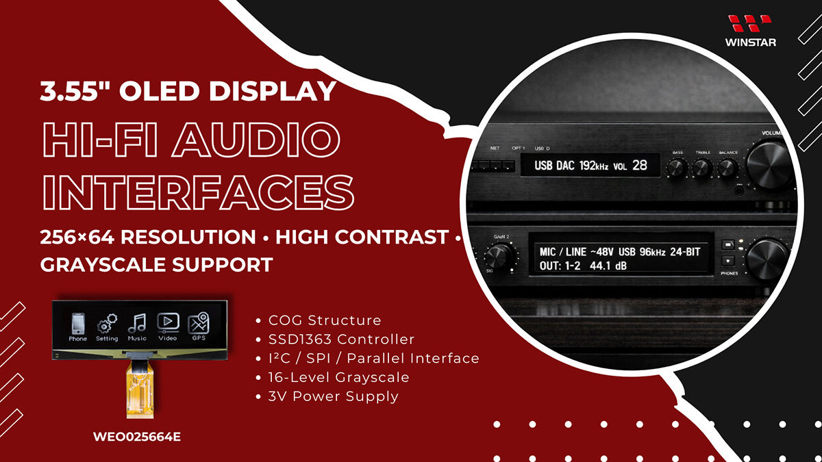
 - WEO025664E")
 - WEO025664E")
 - WEO025664E")
 - WEO025664E")