


我们重视您的隐私
通过点击「允许所有 Cookie」,代表您同意在您的设备上存储 Cookie 以增强网站浏览体验、分析网站使用情况并协助我们的营销和网站效能优化工作。您可以在我们的隐私权政策中找到有关于此的更多信息。


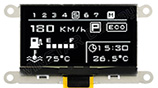
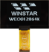
WEO012864G系列是对角线尺寸为2.42寸图形OLED模块,分辨率128x64 像素,模块尺寸为60.5 × 37.0mm,有效区域尺寸为55.01×27.49 mm。此OLED显示屏采用先进的SSD1309 IC,支持多种接口,包括6800、8080、4线SPI和I2C。 此模块的工作温度范围为 -40°C至+80°C,储存温度范围为 -40°C至+85°C。WEO012864G COG绘图型OLED显示屏具有10,000:1 的高对比度度,逻辑电压范围1.65V~3.3V;典型值3.0V。这款OLED显示屏具有高对比度度快、速响应时间、低功耗、多种接口选项和宽工作温度范围等特点使其成为显示高质量影像的绝佳选择,适用于多种产品应用,例如:手持式产品、量测仪器、智能电网、穿戴式产品、物联网设备、医疗设备等等。WEO012864G 2.42寸OLED显示器是任何需要高质量视觉效果、低功耗和多种接口选项的应用的绝佳选择。
华凌光电COG绘图型OLED模块WEO012864G与WEO012864H系列,使用相同的OLED面板但是使用不同的FPC出pin。WEO012864G模块使用ZIF FPC,而WEO012864H则是使用Hot Bar FPC,客户可依据产品应用需求选用适合OLED模块。
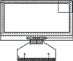
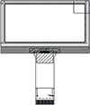
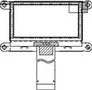
 可另选加铁框 | 可选 FPC
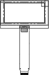
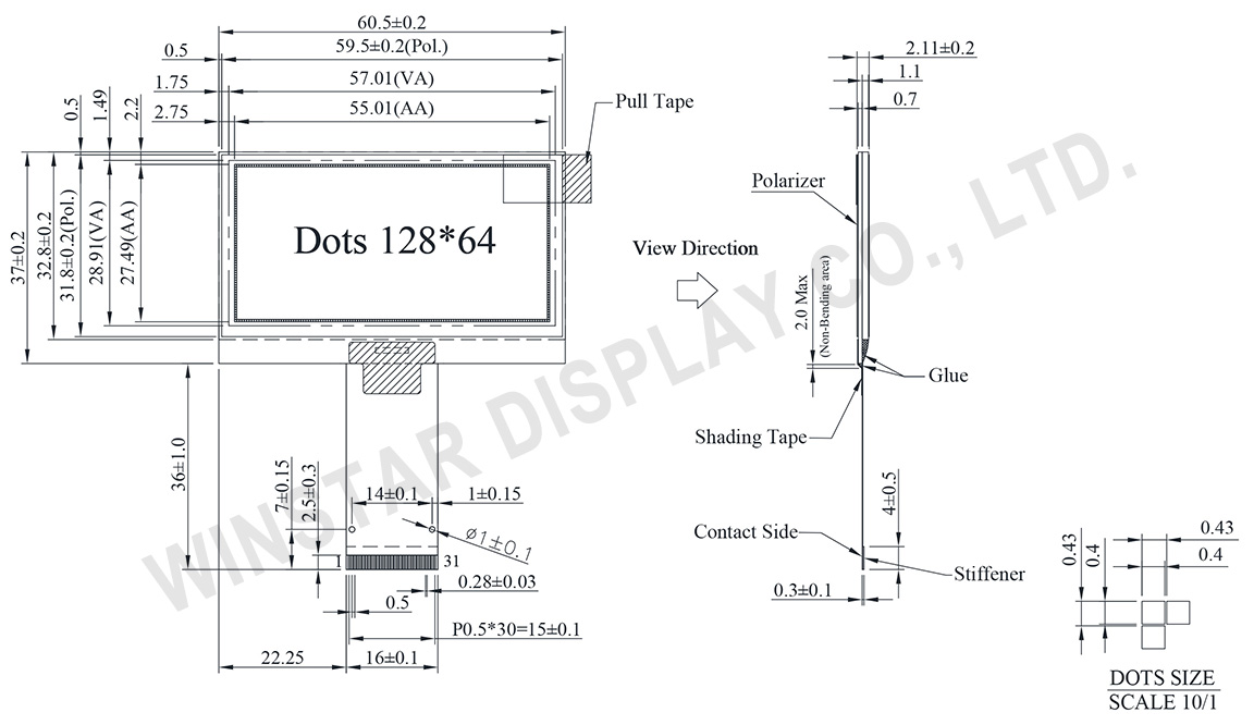
| 项目 | 尺寸 | 单位 |
|---|---|---|
| 点阵 | 128 x 64 | - |
| 模块尺寸 | 60.5 × 37.0 × 2.11 | mm |
| 有效区域 | 55.01 × 27.49 | mm |
| 像素大小 | 0.40 × 0.40 | mm |
| 像素间距 | 0.43 × 0.43 | mm |
| 显示模式 | 被动矩阵 | |
| 发光颜色 | 单色 | |
| 驱动方式 | 1/64 Duty | |
| IC | SSD1309 | |
| 接口 | 6800,8080,4线 SPI,I2C | |
| 尺寸 | 2.42 寸 | |
| 参数 | 符号 | 最小值 | 最大值 | 单位 |
|---|---|---|---|---|
| 逻辑电源电压 | VDD | -0.3 | 4 | V |
| 显示电源电压 | VCC | 0 | 15 | V |
| 工作温度 | TOP | -40 | +80 | °C |
| 储存温度 | TSTG | -40 | +85 | °C |
| 项目 | 符号 | 条件 | 最小值 | 典型值 | 最大值 | 单位 |
|---|---|---|---|---|---|---|
| 逻辑电源电压 | VDD | - | 1.65 | 3.0 | 3.3 | V |
| 显示电源电压 | VCC | - | 7.0 | 13.0 | 13.5 | V |
| 输入高准位 | VIH | - | 0.8×VDD | - | - | V |
| 输入低准位 | VIL | - | - | - | 0.2×VDD | V |
| 输出高准位 | VOH | - | 0.9×VDD | - | - | V |
| 输出低准位 | VOL | - | - | - | 0.1×VDD | V |
| 显示 50% 像素 | ICC | VCC =13V | - | 18 | 27 | mA |
| No. | 符号 | 说明 | |||||||||||||||
|---|---|---|---|---|---|---|---|---|---|---|---|---|---|---|---|---|---|
| 1 | NC(GND) | No connection | |||||||||||||||
| 2 | VSS | Ground. | |||||||||||||||
| 3-10 | NC | No connection | |||||||||||||||
| 11 | VDD | Power supply pin for core logic operation | |||||||||||||||
| 12 | BS1 | MCU bus interface selection pins. Select appropriate logic setting as described in the following table. BS2 and BS1 are pin select
(1) 0 is connected to VSS (2) 1 is connected to VDD |
|||||||||||||||
| 13 | BS2 | ||||||||||||||||
| 14 | NC | No connection | |||||||||||||||
| 15 | CS# | This pin is the chip select input connecting to the MCU. The chip is enabled for MCU communication only when CS# is pulled LOW (active LOW). |
|||||||||||||||
| 16 | RES# | This pin is reset signal input. When the pin is pulled LOW, initialization of the chip is executed. Keep this pin pull HIGH during normal operation. |
|||||||||||||||
| 17 | D/C# | This pin is Data/Command control pin connecting to the MCU. When the pin is pulled HIGH, the data at D[7:0] will be interpreted as data. When the pin is pulled LOW, the data at D[7:0] will be transferred to a command register. In I2C mode, this pin acts as SA0 for slave address selection. |
|||||||||||||||
| 18 | R/W# | This pin is read / write control input pin connecting to the MCU interface. When 6800 interface mode is selected, this pin will be used as Read/Write (R/W#) selection input. Read mode will be carried out when this pin is pulled HIGH and write mode when LOW. When 8080 interface mode is selected, this pin will be the Write (WR#) input. Data write operation is initiated when this pin is pulled LOW and the chip is selected. When serial or I2C interface is selected, this pin must be connected to VSS. |
|||||||||||||||
| 19 | E/RD# | This pin is MCU interface input. When 6800 interface mode is selected, this pin will be used as the Enable (E) signal. Read/write operation is initiated when this pin is pulled HIGH and the chip is selected. When 8080 interface mode is selected, this pin receives the Read (RD#) signal. Read operation is initiated when this pin is pulled LOW and the chip is selected. When serial or I2C interface is selected, this pin must be connected to VSS. |
|||||||||||||||
| 20~27 | D0~D7 | These pins are bi-directional data bus connecting to the MCU data bus. Unused pins are recommended to tie LOW. When serial interface mode is selected, D0 will be the serial clock input: SCLK; D1 will be the serial data input: SDIN and D2 should be kept NC. When I2C mode is selected, D2, D1 should be tied together and serve as SDAout, SDAin in application and D0 is the serial clock input, SCL. |
|||||||||||||||
| 28 | IREF | This pin is the segment output current reference pin. IREF is supplied externally. |
|||||||||||||||
| 29 | VCOMH | COM signal deselected voltage level. A capacitor should be connected between this pin and VSS. |
|||||||||||||||
| 30 | VCC | Power supply for panel driving voltage. This is also the most positive power voltage supply pin. | |||||||||||||||
| 31 | NC(GND) | No connection |
| 图示 | 材质 | 铁框料号 | 详细规格图 | 建立日期 |
|---|---|---|---|---|
 |
SUS-304 | FFL6D00049AA121XXX00 | 检视 | 20160429 |
| 图示 | FPC 全长 | PIN | pitch | ZIF FPC / HOTBAR FPC | 界面 | FPC 料号 | 建立日期 |
|---|---|---|---|---|---|---|---|
 |
37 | 31 | 0.5 | ZIF | 6800,8080,SPI,I2C | FPC2050003111XXXXX01 | 20130625 |
 |
19.75 | 31 | 1 | HOTBAR | 6800,8080,SPI,I2C | FPC2100003101XXXXX02 | 20140220 |
 |
37.15 | 24 | 0.5 | ZIF | 6800,8080,SPI,I2C | FPC2000502411XXXXX01 | 20160803 |
 |
70.85 | 22 | 0.5 | ZIF | 6800,8080,SPI,I2C | FPC2050002211XXXXX03 | 20161228 |
 |
106.57 | 30 | 0.5 | ZIF | 6800,8080,SPI,I2C | FPC2050003011XXXXX11 | 20180620 |

通过点击「允许所有 Cookie」,代表您同意在您的设备上存储 Cookie 以增强网站浏览体验、分析网站使用情况并协助我们的营销和网站效能优化工作。您可以在我们的隐私权政策中找到有关于此的更多信息。