


私たちはあなたのプライバシーを大切にします
「すべてのクッキーを許可」をクリックすると、サイトのナビゲーションを向上させ、サイト使用状況を分析し、マーケティングおよびパフォーマンスの取り組みを支援するために、クッキーをデバイスに保存することに同意したことになります。この件に関する詳細情報は、ポリシーをご覧ください。プライバシーポリシー


Winstar グラフィック表示の有機EL COGのWEO012864HはWEO012864Gと同じの有機ELパネルを使用しておりますが、FPCがHotbarで連結されます。 SSD1309 ICが内蔵され、6800/8080/SPI/I2Cのインターフェースをサポート致します。有機EL・COGモジュールは超薄、軽量、低消費電力のメリットを有して、ハンドヘルド機器、メーター、スマートグリッド、ウェアラブル機器、IoTシステムなどに生かせます。
 Frame Option
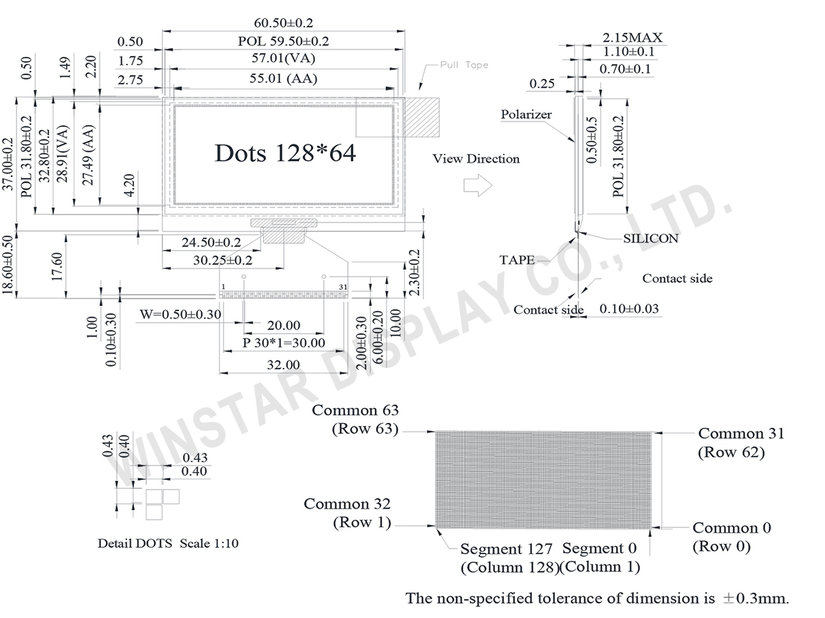
Data source ref:WEO012864HWPP3N00000
| 項目 | 仕様 | 単位 |
|---|---|---|
| ドットマトリックス | 128 x 64 Dots | - |
| モジュールサイズ | 60.5 × 37.0 × 2.15 | mm |
| アクティブエリア | 55.01 × 27.49 | mm |
| ピクセルサイズ | 0.40 × 0.40 | mm |
| ピクセルピッチ | 0.43 × 0.43 | mm |
| 表示モード | パッシブマトリクス(Passive Matrix) | |
| 表示カラー | モノクロ | |
| 駆動方法 | 1/64 Duty | |
| IC | SSD1309 | |
| インターフェイス | 6800, 8080, 4-Wire SPI, I2C | |
| 表示サイズ(対角線) | 2.42 インチ | |
| パラメーター | 記号 | 最小値 | 最大値 | 単位 |
|---|---|---|---|---|
| ロジック電源電圧 | VDD | -0.3 | 4 | V |
| 表示用電源電圧 | VCC | 0 | 15 | V |
| 操作温度 | TOP | -40 | +80 | °C |
| 保存温度 | TSTG | -40 | +85 | °C |
| 項目 | 記号 | 条件 | 最小値 | 典型値 | 最大値 | 単位 |
|---|---|---|---|---|---|---|
| ロジック電源電圧 | VDD | - | 2.8 | 3.0 | 3.3 | V |
| ディスプレイの供給電圧 | VCC | - | 12.5 | 13 | 13.5 | V |
| 高レベル入力 | VIH | - | 0.8×VDD | - | - | V |
| 低レベル入力 | VIL | - | 0 | - | 0.2×VDD | V |
| 高レベル出力 | VOH | - | 0.9×VDD | - | - | V |
| 低レベル出力 | VOL | - | 0 | - | 0.1×VDD | V |
| 50% チェックボード動作電流 | VCC =13.0V | - | 18 | 22 | mA | |
| No. | 記号 | 説明 | |||||||||||||||
|---|---|---|---|---|---|---|---|---|---|---|---|---|---|---|---|---|---|
| 1 | NC(GND) | No connection | |||||||||||||||
| 2 | VCC | Power supply for panel driving voltage. This is also the most positive power voltage supply pin. | |||||||||||||||
| 3 | VCOMH | COM signal deselected voltage level. A capacitor should be connected between this pin and VSS. |
|||||||||||||||
| 4 | IREF | This pin is the segment output current reference pin. IREF is supplied externally. A resistor should be connected between this pin and VSS to maintain the current around 10uA. |
|||||||||||||||
| 5~12 | D7~D0 | These pins are bi-directional data bus connecting to the MCU data bus. Unused pins are recommended to tie LOW. When serial interface mode is selected, D0 will be the serial clock input: SCLK; D1 will be the serial data input: SDIN and D2 should be kept NC. When I2C mode is selected, D2, D1 should be tied together and serve as SDAout, SDAin in application and D0 is the serial clock input, SCL. |
|||||||||||||||
| 13 | E/RD# | This pin is MCU interface input. When 6800 interface mode is selected, this pin will be used as the Enable (E) signal. Read/write operation is initiated when this pin is pulled HIGH and the chip is selected. When 8080 interface mode is selected, this pin receives the Read (RD#) signal. Read operation is initiated when this pin is pulled LOW and the chip is selected. When serial or I2C interface is selected, this pin must be connected to VSS. |
|||||||||||||||
| 14 | R/W# | This pin is read / write control input pin connecting to the MCU interface. When 6800 interface mode is selected, this pin will be used as Read/Write (R/W#) selection input. Read mode will be carried out when this pin is pulled HIGH and write mode when LOW. When 8080 interface mode is selected, this pin will be the Write (WR#) input. Data write operation is initiated when this pin is pulled LOW and the chip is selected. When serial or I2C interface is selected, this pin must be connected to VSS. |
|||||||||||||||
| 15 | D/C# | This pin is Data/Command control pin connecting to the MCU. When the pin is pulled HIGH, the data at D[7:0] will be interpreted as data. When the pin is pulled LOW, the data at D[7:0] will be transferred to a command register. In I2C mode, this pin acts as SA0 for slave address selection. |
|||||||||||||||
| 16 | RES# | This pin is reset signal input. When the pin is pulled LOW, initialization of the chip is executed. Keep this pin pull HIGH during normal operation. |
|||||||||||||||
| 17 | CS# | This pin is the chip select input connecting to the MCU. The chip is enabled for MCU communication only when CS# is pulled LOW (active LOW). |
|||||||||||||||
| 18 | NC | No connection | |||||||||||||||
| 19 | BS2 | MCU bus interface selection pins. Select appropriate logic setting as described in the following table. BS2 and BS1 are pin select
Note (1) 0 is connected to VSS (2) 1 is connected to VDD |
|||||||||||||||
| 20 | BS1 | ||||||||||||||||
| 21 | VDD | Power supply pin for core logic operation | |||||||||||||||
| 22-29 | NC | No connection | |||||||||||||||
| 30 | VSS | Ground. | |||||||||||||||
| 31 | NC(GND) | No connection |

「すべてのクッキーを許可」をクリックすると、サイトのナビゲーションを向上させ、サイト使用状況を分析し、マーケティングおよびパフォーマンスの取り組みを支援するために、クッキーをデバイスに保存することに同意したことになります。この件に関する詳細情報は、ポリシーをご覧ください。プライバシーポリシー