


2.7-inch 128x64 COG OLED Display with PCB and Frame
Model No. WEP012864Q
►Type: Graphic
►Structure: COG + Frame + PCB
►Size: 2.7 inch
►128 x 64 Dot Matrix
►IC:SSD1309
►3V Power supply
►1/64 duty
►Interface: 6800, 8080, SPI, I2C
►Display Color: White / Yellow / Sky Blue / Green
Description
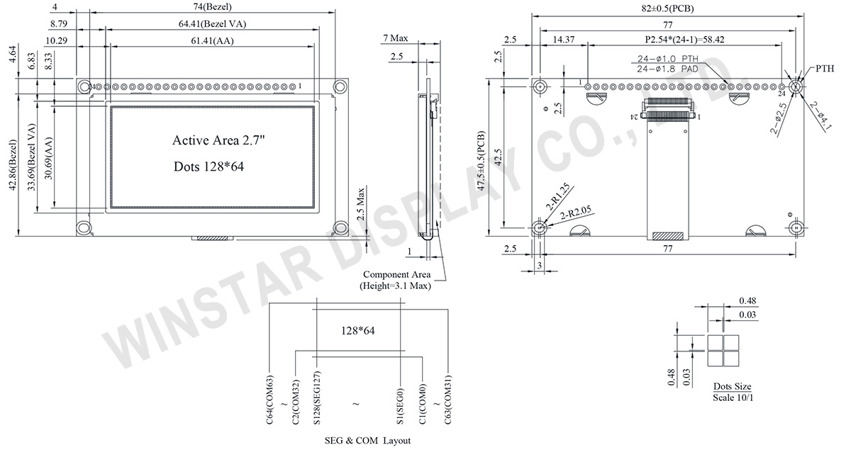
The WEP012864Q series is a 2.7-inch monochrome graphic COG OLED display with a resolution of 128x64 pixels. It incorporates the SSD1309 controller IC and supports communication via 6800 8-bit and 8080 8-bit parallel, I2C, and 4-wire SPI serial interfaces, utilizing a 3V driver. The module dimensions of the WEP012864Q are 82.0 × 47.5 mm, with an active area measuring 61.41 × 30.69 mm. This series shares the same OLED panel as the WEO012864Q and WEF012864Q.
The WEO012864Q is characterized by a frameless design and does not include a PCB.
The WEF012864Q features a frame with four screw holes for added structural stability.
The WEP012864Q distinguishes itself by having both a frame and a PCB, with four screw holes incorporated into the PCB for ease of installation.
These three variants cater to different application requirements, providing options for diverse design considerations and installation preferences.
If there's a need for CTP Touch functionality, please consider the WEP012864Q-CTP model within this series.
The WEP012864Q series is a COG structure OLED display; this OLED module is lightweight, low power, very thin, and features a high contrast ratio of 10,000:1. It is suitable for wall/meter devices, home applications, POS systems, Cloud/IoT systems, intelligent technology devices, energy systems, communication systems, medical instruments, etc.
The WEF012864Q OLED module can operate at temperatures ranging from -40℃ to +80℃, and its storage temperatures range from -40℃ to +80℃.
DRAWING
Data source ref: WEP012864QLPP3N00000
SPECIFICATIONS
Interface Pin Function
| No. | Symbol | Function | |||||||||||||||
|---|---|---|---|---|---|---|---|---|---|---|---|---|---|---|---|---|---|
| 1 | VSS | Ground. | |||||||||||||||
| 2 | VDD | Power supply pin for core logic operation | |||||||||||||||
| 3 | NC | No connection | |||||||||||||||
| 4 | D/C# | ||||||||||||||||
| 5 | R/W# (WR#) |
This pin is read / write control input pin connecting to the MCU interface. When 6800 interface mode is selected, this pin will be used as Read/Write (R/W#) selection input. Read mode will be carried out when this pin is pulled HIGH and write mode when LOW. When 8080 interface mode is selected, this pin will be the Write (WR#) input. Data write operation is initiated when this pin is pulled LOW and the chip is selected. When serial or I2C interface is selected, this pin must be connected to VSS. |
|||||||||||||||
| 6 | E(/RD#) | This pin is MCU interface input. When 6800 interface mode is selected, this pin will be used as the Enable (E) signal. Read/write operation is initiated when this pin is pulled HIGH and the chip is selected. When 8080 interface mode is selected, this pin receives the Read (RD#) signal. Read operation is initiated when this pin is pulled LOW and the chip is selected. When serial or I2C interface is selected, this pin must be connected to VSS. |
|||||||||||||||
| 7-14 | D0~D7 | These pins are bi-directional data bus connecting to the MCU data bus. Unused pins are recommended to tie LOW. When serial interface mode is selected, D0 will be the serial clock input: SCLK; D1 will be the serial data input: SDIN and D2 should be kept NC. When I2C mode is selected, D2, D1 should be tied together and serve as SDAout, SDAin in application and D0 is the serial clock input, SCL. |
|||||||||||||||
| 15 | NC | No connection | |||||||||||||||
| 16 | RES# | This pin is reset signal input. When the pin is pulled LOW, initialization of the chip is executed. Keep this pin pull HIGH during normal operation. |
|||||||||||||||
| 17 | CS# | This pin is the chip select input connecting to the MCU. The chip is enabled for MCU communication only when CS# is pulled LOW (active LOW). |
|||||||||||||||
| 18 | NC | No connection | |||||||||||||||
| 19 | BS2 | MCU bus interface selection pins. Select appropriate logic setting as described in the following table. BS2 and BS1 are pin select
(1) 0 is connected to VSS (2) 1 is connected to VDD |
|||||||||||||||
| 20 | BS1 | ||||||||||||||||
| 21 | NC | No connection | |||||||||||||||
| 22 | NC | No connection | |||||||||||||||
| 23 | NC | No connection | |||||||||||||||
| 24 | NC | No connection |
Mechanical Data
| Item | Dimension | Unit |
|---|---|---|
| Dot Matrix | 128 × 64 | - |
| Module dimension | 82.0 × 47.5 × 7 Max. | mm |
| Active Area | 61.41 × 30.69 | mm |
| Pixel Size | 0.45 × 0.45 | mm |
| Pixel Pitch | 0.48 × 0.48 | mm |
| Display Mode | Passive Matrix | |
| Display Color | Monochrome | |
| Drive Duty | 1/64 Duty | |
| IC | SSD1309 | |
| Interface | 6800,8080,4-Wire SPI,I2C | |
| Size | 2.7 inch | |
Absolute Maximum Ratings
| Parameter | Symbol | Min | Max | Unit |
|---|---|---|---|---|
|
Supply Voltage for Logic |
VDD | -0.3 | 4.0 | V |
|
Operating Temperature |
TOP | -40 | +80 | °C |
|
Storage Temperature |
TSTG | -40 | +85 | °C |
Electronical Characteristics
| Item | Symbol | Condition | Min | Typ | Max | Unit |
|---|---|---|---|---|---|---|
| Supply Voltage for Logic | VDD | - | 2.8 | 3.0 | 3.3 | V |
| High Level Input | VIH | - | 0.8×VDD | - | - | V |
| Low Level Input | VIL | - | - | - | 0.2×VDD | V |
| High Level Output | VOH | - | 0.9×VDD | - | - | V |
| Low Level Output | VOL | - | - | - | 0.1×VDD | V |
| 50% Check Board operating Current | VCC =3V | - | 100 | 200 | mA | |
Search keyword: 128x64 oled, oled 128x64, 2.7 oled, 2.7 inch oled, oled 2.7
