


2,7-Zoll-128x64 COG OLED-Anzeigemodule mit Rahmen, PCB
Modellnummer WEP012864Q
►Typ: Grafik
►Bauweise: COG + Frame + PCB
►Größe: 2,7 Zoll
►128 x 64 Punktmatrix
►IC:SSD1309
►3-V-Stromversorgung
►1/64 duty
►Schnittstelle: 6800, 8080, SPI, I2C
►die Farbe des Displays: Weiß / Gelb / Himmelblau / Grün
Beschreibung
Die WEP012864Q-Serie ist ein 2,7-Zoll monochromatischer COG OLED-Grafikdisplay mit einer Auflösung von 128x64 Pixeln. Es integriert den SSD1309-Controller-IC und unterstützt die Kommunikation über 6800 8-Bit und 8080 8-Bit Parallel, I2C und 4-Draht-SPI-Serienschnittstellen unter Verwendung eines 3V-Treibers. Die Modulabmessungen des WEP012864Q betragen 82,0 × 47,5 mm, mit einer aktiven Fläche von 61,41 × 30,69 mm. Diese Serie teilt dasselbe OLED-Panel wie das WEO012864Q und das WEF012864Q.
Das WEO012864Q zeichnet sich durch ein rahmenloses Design aus und enthält keine Leiterplatte (PCB).
Das WEF012864Q verfügt über einen Rahmen mit vier Schraubenlöchern für zusätzliche strukturelle Stabilität.
Das WEP012864Q unterscheidet sich dadurch, dass es sowohl einen Rahmen als auch eine Leiterplatte (PCB) hat, wobei vier Schraubenlöcher in die Leiterplatte für eine einfache Installation eingearbeitet sind.
Diese drei Varianten erfüllen unterschiedliche Anforderungen und bieten Optionen für vielfältige Designüberlegungen und Installationspräferenzen.
Wenn eine CTP-Touch-Funktionalität erforderlich ist, erwägen Sie das Modell WEP012864Q-CTP innerhalb dieser Serie.
Die WEP012864Q-Serie ist ein COG-Struktur-OLED-Display; dieses OLED-Modul ist leicht, energieeffizient, sehr dünn und weist ein hohes Kontrastverhältnis von 10.000:1 auf. Es eignet sich für Wand-/Messgeräte, Anwendungen im Haushalt, POS-Systeme, Cloud/IoT-Systeme, intelligente Technologiegeräte, Energiesysteme, Kommunikationssysteme, medizinische Instrumente usw.
Das WEF012864Q-OLED-Modul kann bei Temperaturen von -40°C bis +80°C betrieben werden, wobei die Lagertemperaturen von -40°C bis +80°C reichen.
Zeichnung
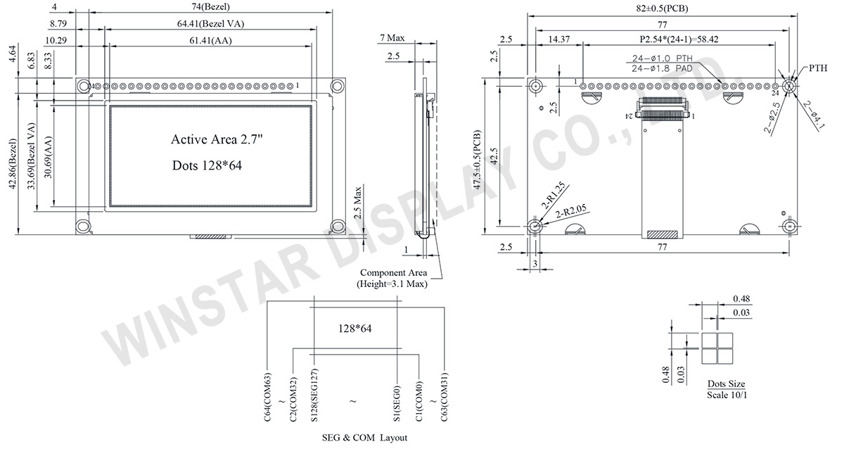
Data source ref: WEP012864QLPP3N00000
Technische Daten
Schnittstelle Pin-Funktion
| No. | Symbol | Beschreibung | |||||||||||||||
|---|---|---|---|---|---|---|---|---|---|---|---|---|---|---|---|---|---|
| 1 | VSS | Ground. | |||||||||||||||
| 2 | VDD | Power supply pin for core logic operation | |||||||||||||||
| 3 | NC | No connection | |||||||||||||||
| 4 | D/C# | ||||||||||||||||
| 5 | R/W# (WR#) |
This pin is read / write control input pin connecting to the MCU interface. When 6800 interface mode is selected, this pin will be used as Read/Write (R/W#) selection input. Read mode will be carried out when this pin is pulled HIGH and write mode when LOW. When 8080 interface mode is selected, this pin will be the Write (WR#) input. Data write operation is initiated when this pin is pulled LOW and the chip is selected. When serial or I2C interface is selected, this pin must be connected to VSS. |
|||||||||||||||
| 6 | E(/RD#) | This pin is MCU interface input. When 6800 interface mode is selected, this pin will be used as the Enable (E) signal. Read/write operation is initiated when this pin is pulled HIGH and the chip is selected. When 8080 interface mode is selected, this pin receives the Read (RD#) signal. Read operation is initiated when this pin is pulled LOW and the chip is selected. When serial or I2C interface is selected, this pin must be connected to VSS. |
|||||||||||||||
| 7-14 | D0~D7 | These pins are bi-directional data bus connecting to the MCU data bus. Unused pins are recommended to tie LOW. When serial interface mode is selected, D0 will be the serial clock input: SCLK; D1 will be the serial data input: SDIN and D2 should be kept NC. When I2C mode is selected, D2, D1 should be tied together and serve as SDAout, SDAin in application and D0 is the serial clock input, SCL. |
|||||||||||||||
| 15 | NC | No connection | |||||||||||||||
| 16 | RES# | This pin is reset signal input. When the pin is pulled LOW, initialization of the chip is executed. Keep this pin pull HIGH during normal operation. |
|||||||||||||||
| 17 | CS# | This pin is the chip select input connecting to the MCU. The chip is enabled for MCU communication only when CS# is pulled LOW (active LOW). |
|||||||||||||||
| 18 | NC | No connection | |||||||||||||||
| 19 | BS2 | MCU bus interface selection pins. Select appropriate logic setting as described in the following table. BS2 and BS1 are pin select
(1) 0 is connected to VSS (2) 1 is connected to VDD |
|||||||||||||||
| 20 | BS1 | ||||||||||||||||
| 21 | NC | No connection | |||||||||||||||
| 22 | NC | No connection | |||||||||||||||
| 23 | NC | No connection | |||||||||||||||
| 24 | NC | No connection |
mechanische Daten
| Artikel | Ausmaß | Einheit |
|---|---|---|
| Punktmatrix | 128 x 64 | dots |
| Abmaße der modul | 82,0 × 47,5 × 7 Max. | mm |
| Aktiver Bereich | 61,41 × 30,69 | mm |
| Punktgröße | 0,45 × 0,45 | mm |
| Punktabstand | 0,48 × 0,48 | mm |
| Display Mode | Passive Matrix | |
| Display Color | Monochrome | |
| Drive Duty | 1/64 Duty | |
| IC | SSD1309 | |
| Schnittstelle | I2C, 4-Wire SPI ,6800, 8080 | |
| Größe | 2,7 Zoll | |
absolute Grenzwerte
| Parameter | Symbol | Mindestwert | Maximalwert | Einheit |
|---|---|---|---|---|
|
Supply Voltage for Logic |
VDD | -0.3 | 4.0 | V |
| Betriebstemperatur | TOP | -40 | +80 | °C |
| Lagertemperatur | TSTG | -40 | +85 | °C |
elektronische Eingenschaften
| Artikel | Symbol | Bedingung | Mindestwert | typischer Wert | Maximalwert | Einheit |
|---|---|---|---|---|---|---|
| Supply Voltage for Logic | VDD | - | 2,8 | 3,0 | 3,3 | V |
| High Level Input | VIH | - | 0,8×VDD | - | - | V |
| Low Level Input | VIL | - | - | - | 0,2×VDD | V |
| High Level Output | VOH | - | 0,9×VDD | - | - | V |
| Low Level Output | VOL | - | - | - | 0,1×VDD | V |
| 50% Check Board operating Current | VCC =3V | - | 100 | 200 | mA | |
