


Display OLED COG 128x64, 2,7 pouces com quadro, PCB
Model No. WEP012864Q
►Tipo: Gráfico
►Estrutura: COG + Frame + PCB
►Tamanho: 2,7 polegadas
►Matriz de pontos 128 x 64
►IC:SSD1309
►Alimentação 3V
►1/64 duty
►Interface: 6800, 8080, SPI, I2C
►Display Color: Branco / Amarelo / Céu azul / Verde
Descrição
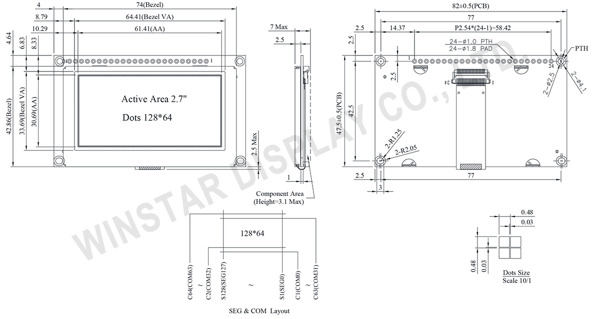
A série WEP012864Q é um visor OLED COG gráfico monocromático de 2,7 polegadas com uma resolução de 128x64 pixels. Ele incorpora o controlador SSD1309 e suporta comunicação via interfaces paralelas de 6800 8 bits e 8080 8 bits, I2C e SPI de 4 fios, utilizando um driver de 3V. As dimensões do módulo do WEP012864Q são 82,0 × 47,5 mm, com uma área ativa de 61,41 × 30,69 mm. Esta série compartilha o mesmo painel OLED que o WEO012864Q e o WEF012864Q.
O WEO012864Q se caracteriza por um design sem moldura e não inclui uma placa de circuito impresso (PCB).
O WEF012864Q apresenta uma estrutura com quatro furos para parafusos para maior estabilidade estrutural.
O WEP012864Q se destaca por ter tanto uma estrutura quanto uma PCB, com quatro furos para parafusos incorporados na PCB para facilitar a instalação.
Essas três variantes atendem a diferentes requisitos de aplicação, fornecendo opções para diversas considerações de design e preferências de instalação.
Se houver necessidade de funcionalidade de toque CTP, por favor, considere o modelo WEP012864Q-CTP dentro desta série.
A série WEP012864Q é um visor OLED de estrutura COG; este módulo OLED é leve, de baixo consumo, muito fino e apresenta uma alta taxa de contraste de 10.000:1. É adequado para dispositivos de parede/medidores, aplicações domésticas, sistemas POS, sistemas Cloud/IoT, dispositivos de tecnologia inteligente, sistemas de energia, sistemas de comunicação, instrumentos médicos, etc.
O módulo OLED WEF012864Q pode operar em temperaturas que variam de -40°C a +80°C, e suas temperaturas de armazenamento variam de -40°C a +80°C.
DRAWING
Data source ref: WEP012864QLPP3N00000
SPECIFICATIONS
Função do pino de interface
| No. | Símbolo | Função | |||||||||||||||
|---|---|---|---|---|---|---|---|---|---|---|---|---|---|---|---|---|---|
| 1 | VSS | Ground. | |||||||||||||||
| 2 | VDD | Power supply pin for core logic operation | |||||||||||||||
| 3 | NC | No connection | |||||||||||||||
| 4 | D/C# | ||||||||||||||||
| 5 | R/W# (WR#) |
This pin is read / write control input pin connecting to the MCU interface. When 6800 interface mode is selected, this pin will be used as Read/Write (R/W#) selection input. Read mode will be carried out when this pin is pulled HIGH and write mode when LOW. When 8080 interface mode is selected, this pin will be the Write (WR#) input. Data write operation is initiated when this pin is pulled LOW and the chip is selected. When serial or I2C interface is selected, this pin must be connected to VSS. |
|||||||||||||||
| 6 | E(/RD#) | This pin is MCU interface input. When 6800 interface mode is selected, this pin will be used as the Enable (E) signal. Read/write operation is initiated when this pin is pulled HIGH and the chip is selected. When 8080 interface mode is selected, this pin receives the Read (RD#) signal. Read operation is initiated when this pin is pulled LOW and the chip is selected. When serial or I2C interface is selected, this pin must be connected to VSS. |
|||||||||||||||
| 7-14 | D0~D7 | These pins are bi-directional data bus connecting to the MCU data bus. Unused pins are recommended to tie LOW. When serial interface mode is selected, D0 will be the serial clock input: SCLK; D1 will be the serial data input: SDIN and D2 should be kept NC. When I2C mode is selected, D2, D1 should be tied together and serve as SDAout, SDAin in application and D0 is the serial clock input, SCL. |
|||||||||||||||
| 15 | NC | No connection | |||||||||||||||
| 16 | RES# | This pin is reset signal input. When the pin is pulled LOW, initialization of the chip is executed. Keep this pin pull HIGH during normal operation. |
|||||||||||||||
| 17 | CS# | This pin is the chip select input connecting to the MCU. The chip is enabled for MCU communication only when CS# is pulled LOW (active LOW). |
|||||||||||||||
| 18 | NC | No connection | |||||||||||||||
| 19 | BS2 | MCU bus interface selection pins. Select appropriate logic setting as described in the following table. BS2 and BS1 are pin select
(1) 0 is connected to VSS (2) 1 is connected to VDD |
|||||||||||||||
| 20 | BS1 | ||||||||||||||||
| 21 | NC | No connection | |||||||||||||||
| 22 | NC | No connection | |||||||||||||||
| 23 | NC | No connection | |||||||||||||||
| 24 | NC | No connection |
Dados Mecânicos
| Item | Dimensão | Unidade |
|---|---|---|
| Matriz de pontos | 128 × 64 | Pontos |
| Dimensão do módulo | 82.0 × 47.5 × 7 Max. | mm |
| Área ativa | 61.41 × 30.69 | mm |
| Tamanho do ponto | 0.45 × 0.45 | mm |
| Distância entre pontos | 0.48 × 0.48 | mm |
| Modo de exibição | Passive Matrix | |
| Cor de exibição | Monochrome | |
| Drive Duty | 1/64 Duty | |
| IC | SSD1309 | |
| Interface | I2C, 4-Wire SPI ,6800, 8080 | |
| Tamanho | 2,7 polegadas | |
Classificações Máximas Absolutas
| Parameter | Símbolo | Valor Min | Valor Máximo | Unidade |
|---|---|---|---|---|
| Supply Voltage for Logic | VDD | -0.3 | 4.0 | V |
| Temperatura de operação | TOP | -40 | +80 | °C |
| Temperatura de armazenamento | TSTG | -40 | +85 | °C |
Características Eletrônicas
| Item | Símbolo | Condição | Valor Min | Valor Típico | Valor Máximo | Unidade |
|---|---|---|---|---|---|---|
| Supply Voltage for Logic | VDD | - | 2.8 | 3.0 | 3.3 | V |
| High Level Input | VIH | - | 0.8×VDD | - | - | V |
| Low Level Input | VIL | - | - | - | 0.2×VDD | V |
| High Level Output | VOH | - | 0.9×VDD | - | - | V |
| Low Level Output | VOL | - | - | - | 0.1×VDD | V |
| 50% Check Board operating Current | VCC =3V | - | 100 | 200 | mA | |
