


2.7 pollici 128x64 COG+FR+PCB OLED Moduli Display
Modello numero WEP012864Q
►Tipo: grafico
►Struttura: COG + cornice + PCB
►Dimensione: 2.7 pollici
►128 x 64 a matrice di punti
►IC:SSD1309
►Alimentatore 3V
►1/64 duty
►Interfaccia: 6800, 8080, SPI, I2C
►Colore display: Bianco / Giallo / Cielo blu / Verde
Descrizione
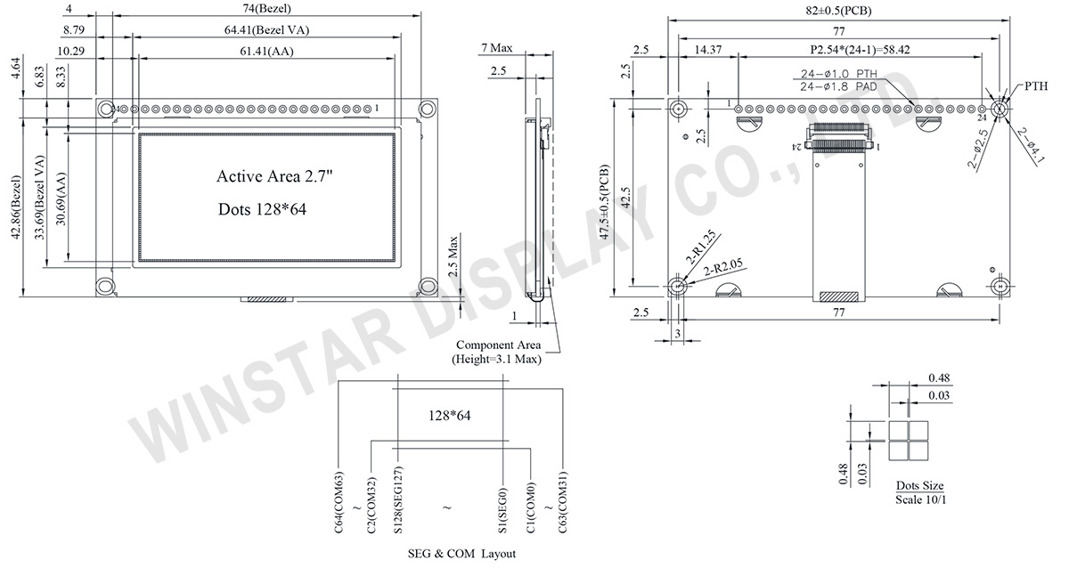
La serie WEP012864Q è un display OLED grafico COG da 2.7 pollici in scala di grigi con una risoluzione di 128x64 pixel. Incorpora il controller IC SSD1309 e supporta la comunicazione tramite interfacce parallele a 8 bit 6800 e 8080, I2C e SPI a 4 fili, utilizzando un driver a 3V. Le dimensioni del modulo del WEP012864Q sono di 82.0 × 47.5 mm, con un'area attiva di 61.41 × 30.69 mm. Questa serie condivide lo stesso pannello OLED del WEO012864Q e del WEF012864Q.
Il WEO012864Q si caratterizza per un design senza cornice e non include una scheda PCB.
Il WEF012864Q presenta una cornice con quattro fori per viti per una maggiore stabilità strutturale.
Il WEP012864Q si distingue per avere sia una cornice che una scheda PCB, con quattro fori per viti incorporati nella scheda PCB per facilitare l'installazione.
Queste tre varianti soddisfano diverse esigenze applicative, offrendo opzioni per diverse considerazioni di progettazione e preferenze di installazione.
Se è necessaria la funzionalità CTP Touch, prendere in considerazione il modello WEP012864Q-CTP all'interno di questa serie.
La serie WEP012864Q è un display OLED di struttura COG; questo modulo OLED è leggero, a basso consumo, molto sottile e presenta un alto rapporto di contrasto di 10.000:1. È adatto per dispositivi da parete/metro, applicazioni domestiche, sistemi POS, sistemi Cloud/IoT, dispositivi tecnologici intelligenti, sistemi energetici, sistemi di comunicazione, strumenti medici, ecc.
Il modulo OLED WEF012864Q può operare a temperature comprese tra -40°C e +80°C, mentre la temperatura di conservazione varia da -40°C a +80°C.
DISEGNO
Data source ref: WEP012864QLPP3N00000
SPECIFICHE TECNICHE
Funzione dei Pin di Interfaccia
| No. | Simbolo | Funzione | |||||||||||||||
|---|---|---|---|---|---|---|---|---|---|---|---|---|---|---|---|---|---|
| 1 | VSS | Ground. | |||||||||||||||
| 2 | VDD | Power supply pin for core logic operation | |||||||||||||||
| 3 | NC | No connection | |||||||||||||||
| 4 | D/C# | ||||||||||||||||
| 5 | R/W# (WR#) |
This pin is read / write control input pin connecting to the MCU interface. When 6800 interface mode is selected, this pin will be used as Read/Write (R/W#) selection input. Read mode will be carried out when this pin is pulled HIGH and write mode when LOW. When 8080 interface mode is selected, this pin will be the Write (WR#) input. Data write operation is initiated when this pin is pulled LOW and the chip is selected. When serial or I2C interface is selected, this pin must be connected to VSS. |
|||||||||||||||
| 6 | E(/RD#) | This pin is MCU interface input. When 6800 interface mode is selected, this pin will be used as the Enable (E) signal. Read/write operation is initiated when this pin is pulled HIGH and the chip is selected. When 8080 interface mode is selected, this pin receives the Read (RD#) signal. Read operation is initiated when this pin is pulled LOW and the chip is selected. When serial or I2C interface is selected, this pin must be connected to VSS. |
|||||||||||||||
| 7-14 | D0~D7 | These pins are bi-directional data bus connecting to the MCU data bus. Unused pins are recommended to tie LOW. When serial interface mode is selected, D0 will be the serial clock input: SCLK; D1 will be the serial data input: SDIN and D2 should be kept NC. When I2C mode is selected, D2, D1 should be tied together and serve as SDAout, SDAin in application and D0 is the serial clock input, SCL. |
|||||||||||||||
| 15 | NC | No connection | |||||||||||||||
| 16 | RES# | This pin is reset signal input. When the pin is pulled LOW, initialization of the chip is executed. Keep this pin pull HIGH during normal operation. |
|||||||||||||||
| 17 | CS# | This pin is the chip select input connecting to the MCU. The chip is enabled for MCU communication only when CS# is pulled LOW (active LOW). |
|||||||||||||||
| 18 | NC | No connection | |||||||||||||||
| 19 | BS2 | MCU bus interface selection pins. Select appropriate logic setting as described in the following table. BS2 and BS1 are pin select
(1) 0 is connected to VSS (2) 1 is connected to VDD |
|||||||||||||||
| 20 | BS1 | ||||||||||||||||
| 21 | NC | No connection | |||||||||||||||
| 22 | NC | No connection | |||||||||||||||
| 23 | NC | No connection | |||||||||||||||
| 24 | NC | No connection |
Dati meccanici
| Articolo | Dimensioni | Unità |
|---|---|---|
| A matrice di punti | 128 × 64 | dots |
| Dimensione del modulo | 82.0 × 47.5 × 7 Max. | mm |
| Area attiva | 61.41 × 30.69 | mm |
| Dimensioni del Dot | 0.45 × 0.45 | mm |
| Passo del Dot | 0.48 × 0.48 | mm |
| Modalità display | Matrice passiva | |
| Colore display | Monocromatici | |
| Drive Duty | 1/64 Duty | |
| IC | SSD1309 | |
| Interfaccia | I2C, 4-Wire SPI ,6800, 8080 | |
| Dimension | 2.7 pollici | |
Valori massimi assoluti
| Parameter | Simbolo | Valore Min | Valore massimo | Unità |
|---|---|---|---|---|
|
Supply Voltage for Logic |
VDD | -0.3 | 4.0 | V |
| Temperatura di lavoro | TOP | -40 | +80 | °C |
| Temperatura di stock | TSTG | -40 | +85 | °C |
Caratteristiche elettriche
| Articolo | Simbolo | Condizione | Valore Min | Valore tipico | Valore massimo | Unità |
|---|---|---|---|---|---|---|
| Supply Voltage for Logic | VDD | - | 2.8 | 3.0 | 3.3 | V |
| High Level Input | VIH | - | 0.8×VDD | - | - | V |
| Low Level Input | VIL | - | - | - | 0.2×VDD | V |
| High Level Output | VOH | - | 0.9×VDD | - | - | V |
| Low Level Output | VOL | - | - | - | 0.1×VDD | V |
| 50% Check Board operating Current | VCC =3V | - | 100 | 200 | mA | |
Search keyword: 128x64 oled, oled 128x64, 2.7 oled, 2.7 pollici oled, oled 2.7
