 - WFM0108A2TAJASNN000")
 - WF18HSLAADNN0")
 - WL0F00050000FGAADSA00")


我們重視您的隱私
通過點擊「允許所有 Cookie」,代表您同意在您的設備上存儲 Cookie 以增強網站瀏覽體驗、分析網站使用情況並協助我們的行銷和網站效能優化工作。您可以在我們的隱私權政策中找到有關於此的更多資訊。


型號 WFN0240A2TBNADNN000
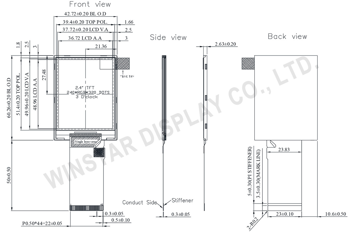
►尺寸: 2.4吋
►解析度: 240 x 320 像素
►視角: 3H
►介面: MCU / SPI / SPI+RGB
►驅動IC:ST7789
►控制板: 無
►亮度(cd/m²): 250
►鐵框螺絲孔: 無
►觸控面板: 無
WFN0240A2TBNADNN000 為一款 2.4 吋 Transflective(半透反射式)TFT-LCD 顯示模組,適用於室內與戶外不同光源環境下的穩定顯示需求。此模組具備 240×320 解析度,並搭載 ST7789 驅動 IC,可提供穩定且一致的顯示效能。
本產品支援多種介面,包括 8/9/16/18-bit MCU、3-line/4-line serial 以及 3/4 SPI + 16/18-bit RGB,有助於系統整合與設計彈性。模組表面採用 防眩光處理,操作溫度範圍為 -20℃ 至 +70℃,適用於手持式裝置、工業控制設備與醫療應用等需具備良好可視性與可靠性的場景。

| 項目 | 規格 | 單位 |
|---|---|---|
| 尺寸 | 2.4 | 吋 |
| 解析度 | 240 × RGB × 320(TFT) | dots |
| 模組尺寸 | 42.72 × 60.26 × 2.63 | mm |
| 有效區域 | 36.72 × 48.96 | mm |
| 像素間距 | 0.153 × 0.153 | mm |
| LCD類型 | TFT, 白色,半透射式 | |
| 視角 | 3點鐘方向 | |
| TFT介面 | 8/9/16/18Bit MCU 3/4SPI+16/18Bit RGB 3-line/4-line Serial |
|
| 背光類型 | LED ,平常白 | |
| TFT驅動IC | ST7789 或相容IC | |
| 觸控面板 | 無觸控面板 | |
| 表面 | 防眩光 | |
| 項目 | 符號 | 最小值 | 典型值 | 最大值 | 單位 |
|---|---|---|---|---|---|
| 工作溫度 | TOP | -20 | - | +60 | ℃ |
| 儲存溫度 | TST | -30 | - | +70 | ℃ |
| 項目 | 符號 | 最小值 | 典型值 | 最大值 | 單位 |
|---|---|---|---|---|---|
| 數位電源電壓 | VCC | 2.4 | 3.3 | 3.6 | V |
| 邏輯電壓 | IOVCC | 1.65 | 1.8 | 3.3 | V |
| 正常模式工作電流 | IDD | -- | 5 | 10 | mA |
| 輸入電壓 | VIH | 0.7 IOVCC | IOVCC | V | |
| VIL | GND | 0.3 IOVCC | V | ||
| 輸出電壓 | VOH | 0.8 IOVCC | IOVCC | V | |
| VOL | GND | 0.2 IOVCC | V |
| 項目 | 符號 | 最小值 | 典型值 | 最大值 | 單位 |
|---|---|---|---|---|---|
| LED電流 | - | - | 80 | - | mA |
| LED電壓 | VLEDA | 2.7 | 3.1 | 3.3 | V |
| LED使用壽命 | - | 50,000 | - | - | Hr |
| Pin No | 符號 | 說明 | I/O |
|---|---|---|---|
| 1 | NC | No connection | -- |
| 2 | NC | No connection | -- |
| 3 | NC | No connection | -- |
| 4 | NC | No connection | -- |
| 5 | GND | Ground. | P |
| 6 | GND | Ground. | P |
| 7 | VCC | Supply voltage(3.3V). | I |
| 8 | VCC | Supply voltage(3.3V). | I |
| 9 | IOVCC | Power Supply for I/O System. | I |
| 10 | SDO | SPI interface output pin. -The data is output on the falling edge of the SCL signal. -If not used, let this pin open. |
O |
| 11-28 | DB17-DB0 | 18-bit parallel bi-directional data bus for MCU system and RGB i nterface mode. Fix to GND level when not in use |
I/O |
| 29 | DIN(SDA) | Serial input signal. The data is latched on the rising edge of the SCL signal. fix this pin at IOVCC or GND when not in use. |
I/O |
| 30 | PCLK | Dot clock signal for RGB interface operation. Fix this pin at IOVCC or GND when not in use. |
I |
| 31 | DE | Data enable signal for RGB interface operation. fix this pin at IOVCC or GND when not in use. |
I |
| 32 | HSYNC | Line synchronizing signal for RGB interface operation. fix this pin at IOVCC or GND when not in use. |
I |
| 33 | VSYNC | Frame synchronizing signal for RGB interface operation. fix this pin at IOVCC or GND when not in use. |
I |
| 34 | RD | Read enable in 8080 MCU parallel interface. -If not used, please fix this pin at IOVCC or DGND. |
I |
| 35 | WR(SPI-RS) | -Write enable in MCU parallel interface. Display data/command selection pin in 4-line serial interface. Second Data lane in 2 data lane serial interface. -If not used, please fix this pin at IOVCC or DGND. |
I |
| 36 | RS(SPI-SCL) | -Display data/command selection pin in parallel interface. -This pin is used to be serial interface clock. RS=’1’: display data or parameter. RS=’0’: command data. -If not used, please fix this pin at IOVCC or DGND. |
I |
| 37 | CS | Chip select input pin (“Low” enable). fix this pin at IOVCC or GND when not in use. |
I |
| 38 | RESET | This signal will reset the device and must be applied to properly initialize the chip. |
I |
| 39 | IM0 | 18-bit parallel bi-directional data bus for MCU system and RGB interface mode. Fix to GND level when not in use |
I |
| 40 | IM1 | ||
| 41 | IM2 | ||
| 42 | NC | No connection | - |
| 43 | LEDA | Anode pin of backlight | P |
| 44 | NC | No connection | - |
| 45 | LEDK | Cathode pin OF backlight | P |
| IM2 | IM1 | IM0 | Interface type | DB Pin in use |
|---|---|---|---|---|
| 0 | 0 | 0 | 80-16bit interface | DB17-DB10,DB8-DB1 |
| 0 | 0 | 1 | 80-8bit interface | DB17-DB10 |
| 0 | 1 | 0 | 80-18bit interface | DB17-DB0 |
| 0 | 1 | 1 | 80~9bit interface | DB17-DB9 |
| 1 | 0 | 1 | 3-Wire 9bit data serial interface. | SDA SCL CS |
| 1 | 1 | 0 | 4-Wire 8bit data serial interface | SDA SCL CS RS |

通過點擊「允許所有 Cookie」,代表您同意在您的設備上存儲 Cookie 以增強網站瀏覽體驗、分析網站使用情況並協助我們的行銷和網站效能優化工作。您可以在我們的隱私權政策中找到有關於此的更多資訊。