


私たちはあなたのプライバシーを大切にします
「すべてのクッキーを許可」をクリックすると、サイトのナビゲーションを向上させ、サイト使用状況を分析し、マーケティングおよびパフォーマンスの取り組みを支援するために、クッキーをデバイスに保存することに同意したことになります。この件に関する詳細情報は、ポリシーをご覧ください。プライバシーポリシー


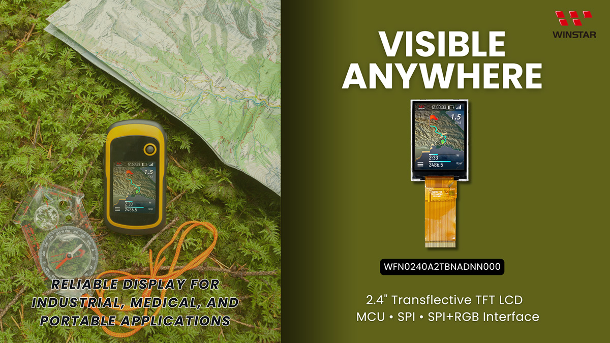
型番 WFN0240A2TBNADNN000
►サイズ: 2.4インチ
►解像度: 240 x 320 ピクセル
►視野角: 3H
►インターフェース: MCU / SPI / SPI+RGB
►駆動IC:ST7789
►コントロールボード: 無
►輝度(cd/m²): 250
►スルーホールフレーム: 無
►タッチパネル: 無
WFN0240A2TBNADNN000 は、屋内外のさまざまな照明環境に対応した 2.4インチのトランスフレクティブ(半透過反射型)TFT-LCDモジュールです。240×320 解像度とST7789 ドライバICを搭載し、安定した表示性能を実現します。
本製品は、8/9/16/18-bit MCU、3-line/4-line シリアル、および 3/4 SPI + 16/18-bit RGB インターフェースに対応しており、システム設計の柔軟性を高めます。さらに、アンチグレア表面処理を採用し、動作温度範囲は -20℃~+70℃ に対応。ハンディ端末、産業機器、医療機器など、高い視認性と信頼性が求められる用途に適しています。
| 項目 | 仕様 | 単位 |
|---|---|---|
| サイズ | 2.4 | インチ |
| ドットマトリックス | 240 × RGB × 320(TFT) | dots |
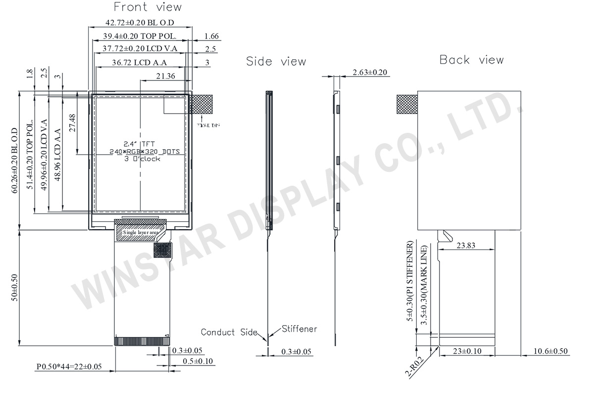
| 外形寸法 | 42.72 × 60.26 × 2.63 | mm |
| 有効エリア | 36.72 × 48.96 | mm |
| ドットピッチ | 0.153 × 0.153 | mm |
| LCDタイプ | TFT・白色・半透過型 | |
| 視野角度 | 3 時間 | |
| TFT インターフェイス | 8/9/16/18Bit MCU 3/4SPI+16/18Bit RGB 3-line/4-line Serial |
|
| バックライトタイプ | LED・ノーマリ・ホワイト | |
| ドライバIC | ST7789或いは互換性コントローラー | |
| タッチパネル | タッチパネル無し | |
| 表面処理 | アンチグレア | |
| 項目 | 記号 | 最小値 | 標準値 | 最大値 | 単位 |
|---|---|---|---|---|---|
| 操作温度 | TOP | -20 | - | +60 | ℃ |
| 保存温度 | TST | -30 | - | +70 | ℃ |
| 項目 | 記号 | 最小値 | 標準値 | 最大値 | 単位 |
|---|---|---|---|---|---|
| デジタル供給電圧 | VCC | 2.4 | 3.3 | 3.6 | V |
| ロジック電源 | IOVCC | 1.65 | 1.8 | 3.3 | V |
| ノーマルモード動作電流 | IDD | -- | 5 | 10 | mA |
| 入力電圧レベル | VIH | 0.7 IOVCC | IOVCC | V | |
| VIL | GND | 0.3 IOVCC | V | ||
| 出力電圧レベル | VOH | 0.8 IOVCC | IOVCC | V | |
| VOL | GND | 0.2 IOVCC | V |
| 項目 | 記号 | 最小値 | 標準値 | 最大値 | 単位 |
|---|---|---|---|---|---|
| LED電流 | - | - | 80 | - | mA |
| LED電圧 | VLEDA | 2.7 | 3.1 | 3.3 | V |
| LEDの寿命 | - | 50,000 | - | - | Hr |
| Pin No | 記号 | 功能 | I/O |
|---|---|---|---|
| 1 | NC | No connection | -- |
| 2 | NC | No connection | -- |
| 3 | NC | No connection | -- |
| 4 | NC | No connection | -- |
| 5 | GND | Ground. | P |
| 6 | GND | Ground. | P |
| 7 | VCC | Supply voltage(3.3V). | I |
| 8 | VCC | Supply voltage(3.3V). | I |
| 9 | IOVCC | Power Supply for I/O System. | I |
| 10 | SDO | SPI interface output pin. -The data is output on the falling edge of the SCL signal. -If not used, let this pin open. |
O |
| 11-28 | DB17-DB0 | 18-bit parallel bi-directional data bus for MCU system and RGB i nterface mode. Fix to GND level when not in use |
I/O |
| 29 | DIN(SDA) | Serial input signal. The data is latched on the rising edge of the SCL signal. fix this pin at IOVCC or GND when not in use. |
I/O |
| 30 | PCLK | Dot clock signal for RGB interface operation. Fix this pin at IOVCC or GND when not in use. |
I |
| 31 | DE | Data enable signal for RGB interface operation. fix this pin at IOVCC or GND when not in use. |
I |
| 32 | HSYNC | Line synchronizing signal for RGB interface operation. fix this pin at IOVCC or GND when not in use. |
I |
| 33 | VSYNC | Frame synchronizing signal for RGB interface operation. fix this pin at IOVCC or GND when not in use. |
I |
| 34 | RD | Read enable in 8080 MCU parallel interface. -If not used, please fix this pin at IOVCC or DGND. |
I |
| 35 | WR(SPI-RS) | -Write enable in MCU parallel interface. Display data/command selection pin in 4-line serial interface. Second Data lane in 2 data lane serial interface. -If not used, please fix this pin at IOVCC or DGND. |
I |
| 36 | RS(SPI-SCL) | -Display data/command selection pin in parallel interface. -This pin is used to be serial interface clock. RS=’1’: display data or parameter. RS=’0’: command data. -If not used, please fix this pin at IOVCC or DGND. |
I |
| 37 | CS | Chip select input pin (“Low” enable). fix this pin at IOVCC or GND when not in use. |
I |
| 38 | RESET | This signal will reset the device and must be applied to properly initialize the chip. |
I |
| 39 | IM0 | 18-bit parallel bi-directional data bus for MCU system and RGB interface mode. Fix to GND level when not in use |
I |
| 40 | IM1 | ||
| 41 | IM2 | ||
| 42 | NC | No connection | - |
| 43 | LEDA | Anode pin of backlight | P |
| 44 | NC | No connection | - |
| 45 | LEDK | Cathode pin OF backlight | P |
| IM2 | IM1 | IM0 | Interface type | DB Pin in use |
|---|---|---|---|---|
| 0 | 0 | 0 | 80-16bit interface | DB17-DB10,DB8-DB1 |
| 0 | 0 | 1 | 80-8bit interface | DB17-DB10 |
| 0 | 1 | 0 | 80-18bit interface | DB17-DB0 |
| 0 | 1 | 1 | 80~9bit interface | DB17-DB9 |
| 1 | 0 | 1 | 3-Wire 9bit data serial interface. | SDA SCL CS |
| 1 | 1 | 0 | 4-Wire 8bit data serial interface | SDA SCL CS RS |

「すべてのクッキーを許可」をクリックすると、サイトのナビゲーションを向上させ、サイト使用状況を分析し、マーケティングおよびパフォーマンスの取り組みを支援するために、クッキーをデバイスに保存することに同意したことになります。この件に関する詳細情報は、ポリシーをご覧ください。プライバシーポリシー