我們重視您的隱私
通過點擊「允許所有 Cookie」,代表您同意在您的設備上存儲 Cookie 以增強網站瀏覽體驗、分析網站使用情況並協助我們的行銷和網站效能優化工作。您可以在我們的隱私權政策中找到有關於此的更多資訊。

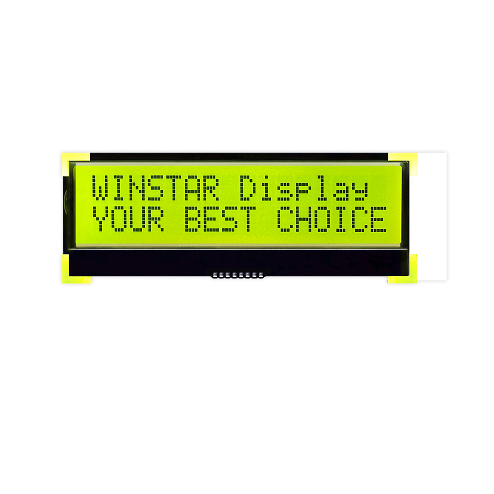
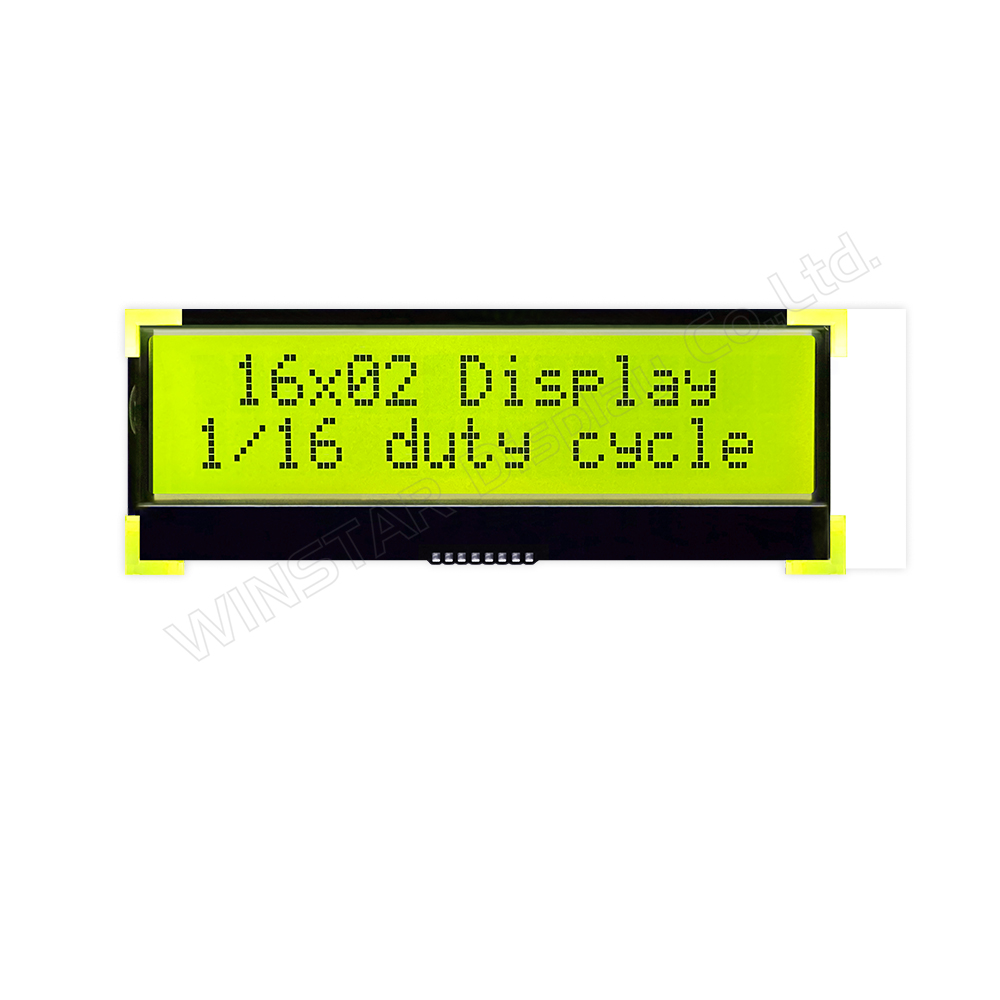
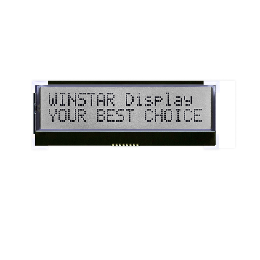
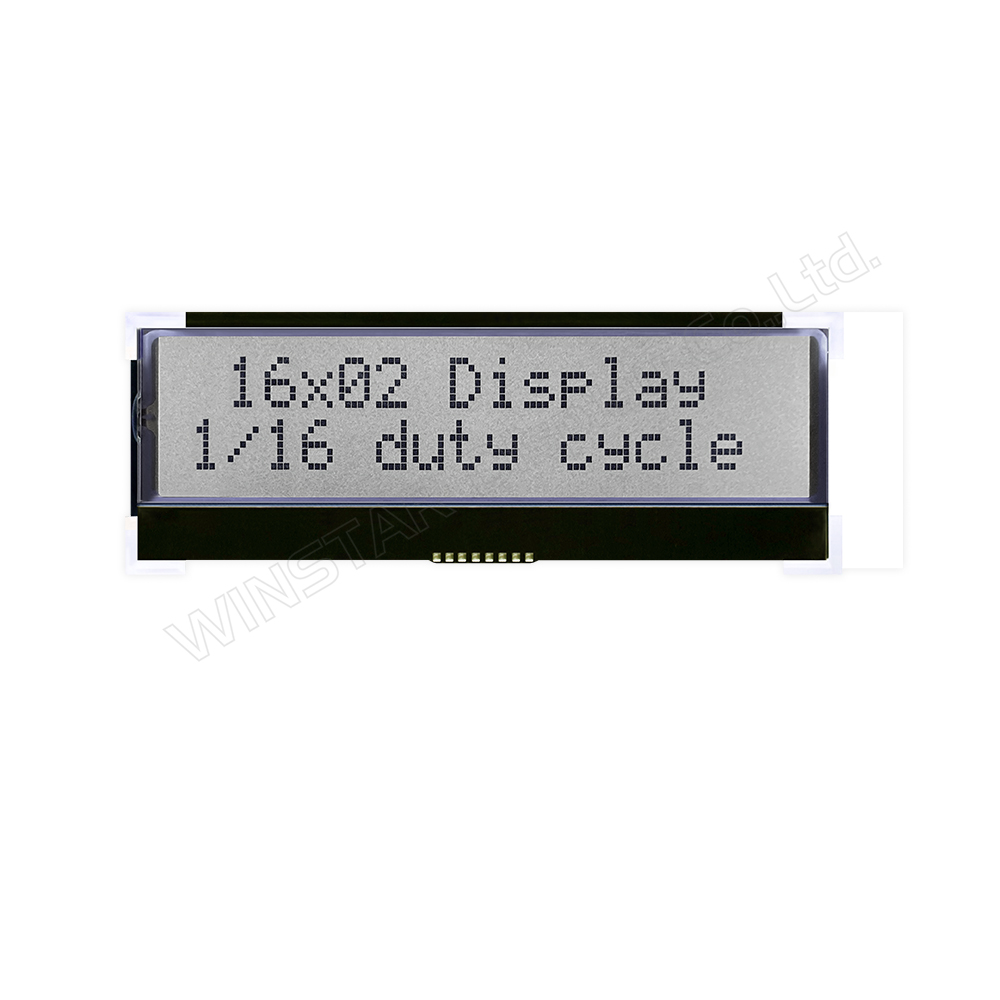
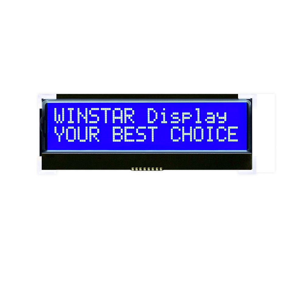
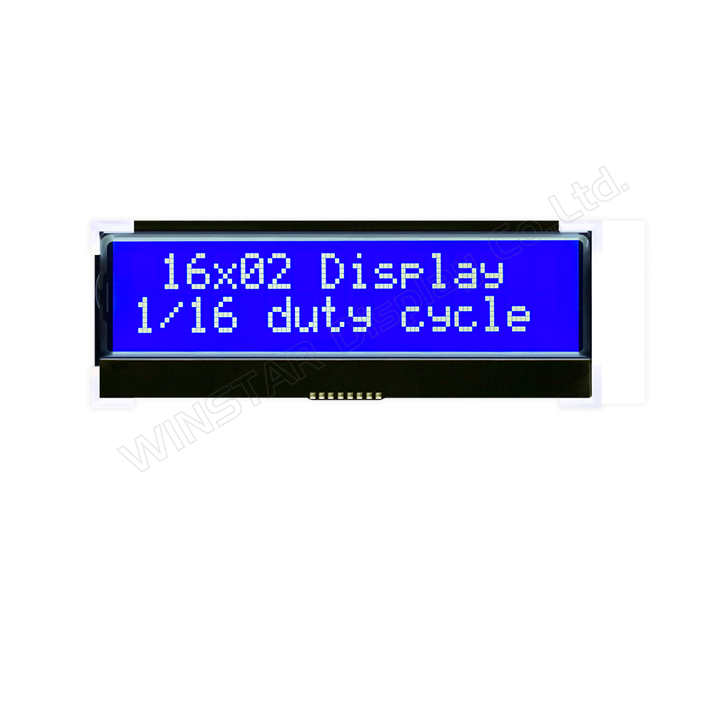
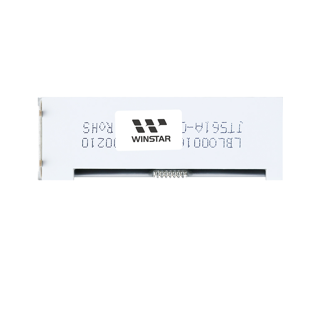
WO1602K 為16x2 COG 字元 LCD 顯示模組,採用金屬針腳設計,搭載 I2C 介面及 ST7032Ai 控制 IC。模組支援 3 V 與 5 V 邏輯電源(VDD),採用 1/16 Duty 驅動方式。
模組尺寸為 74.2 x 25.2 x 6.3 mm,可視區尺寸為 61.0 x 15.1 mm,有效顯示區尺寸為 56.2 x 11.5 mm。COG(Chip-on-Glass)結構設計使其適用於手持式裝置、可攜式儀器、測試設備、工業控制系統及各類嵌入式應用。
WO1602K 模組工作溫度範圍為 -20℃ ~ +70℃,儲存溫度範圍為 -30℃ ~ +80℃。WO1602K 亦可作為 WO1602G 的替代方案,適用於 ST7032Ai 控制 IC 規格需求,或因 IC 供應短缺及交期較長時的替代選擇。
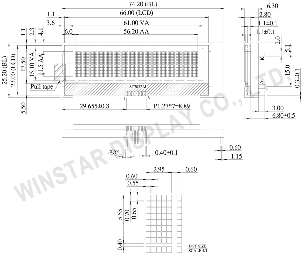
| 項目 | 規格 | 單位 |
|---|---|---|
| 字元數 | 16字 x 2行 | - |
| 模組尺寸 | 74.2 x 25.2 x 6.3 | mm |
| 檢視區域 | 61.0 x 15.1 | mm |
| 有效區域 | 56.2 x 11.5 | mm |
| 點大小 | 0.55 x 0.65 | mm |
| 點間距 | 0.60 x 0.70 | mm |
| 字元大小 | 2.95 x 5.55 | mm |
| 字元間距 | 3.55 x 5.95 | mm |
| 驅動方式 | 1/16 Duty , 1/5 Bias | |
| 背光類型 | LED | |
| IC | ST7032Ai | |
| 介面 | I2C | |
| 項目 | 符號 | 最小值 | 標準值 | 最大值 | 單位 |
|---|---|---|---|---|---|
| 工作溫度 | TOP | -20 | - | +70 | ℃ |
| 儲存溫度 | TST | -30 | - | +80 | ℃ |
| 輸入電壓 | VIN | -0.3 | - | VDD+0.3 | V |
| 電源電壓 | VDD-VSS | -0.3 | - | +4.0 | V |
| LCD驅動電壓 | VLCD | -0.3 | - | 7.0 | V |
| 項目 | 符號 | 條件 | 最小值 | 標準值 | 最大值 | 單位 |
|---|---|---|---|---|---|---|
| 邏輯電源電壓 | VDD-VSS | - | 2.7 | 3.0 | 3.3 | V |
| LCD電源電壓 | VLCD | Ta=-20℃ Ta=25℃ Ta=70℃ |
- 4.3 - |
- 4.5 - |
- 4.7 - |
V V V |
| 輸入高電壓 | VIH | - | 0.7 VDD | - | VDD | V |
| 輸入低電壓 | VIL | - | VDD | - | 0.3 VDD | V |
| 供電電流 | IDD | - | - | 1.0 | - | mA |
| Pin No. | 符號 | 說明 |
|---|---|---|
| 1 | VG | VG is the LCD driving voltage for segment circuits. VGO is the output of VG regulator. VGS is the feedback of VG regulator. VGI is the VG input of segment circuits. 1.6 ≤ VG < VDD2. |
| 2 | XV0 | XV0 is the LCD driving voltage for common circuits at positive frame. XV0OUT is the output of XV0 regulator. XV0S is the feedback of XV0 regulator. XV0I is the V0 input of common circuits |
| 3 | V0 | V0 is the LCD driving voltage for common circuits at negative frame. V0OUT is the output of V0 regulator. V0S is the feedback of V0 regulator. V0I is the V0 input of common circuits. Be sure that: V0 ≥ VG > VM > VSS ≥ XV0 (under operation). |
| 4 | VDD | Power supply input. |
| 5 | VSS | Ground |
| 6 | SDA | Serial data input |
| 7 | SCL | Serial clock input |
| 8 | RST | Hardware reset input pin. When RSTB is “L”, internal initialization is executed and the internal registers will be initialized. |


通過點擊「允許所有 Cookie」,代表您同意在您的設備上存儲 Cookie 以增強網站瀏覽體驗、分析網站使用情況並協助我們的行銷和網站效能優化工作。您可以在我們的隱私權政策中找到有關於此的更多資訊。