我们重视您的隐私
通过点击「允许所有 Cookie」,代表您同意在您的设备上存储 Cookie 以增强网站浏览体验、分析网站使用情况并协助我们的营销和网站效能优化工作。您可以在我们的隐私权政策中找到有关于此的更多信息。
 - WO1602K")
 - WO1602K")
 - WO1602K")
 - WO1602K")
 - WO1602K")
 - WO1602K")
 - WO1602K")
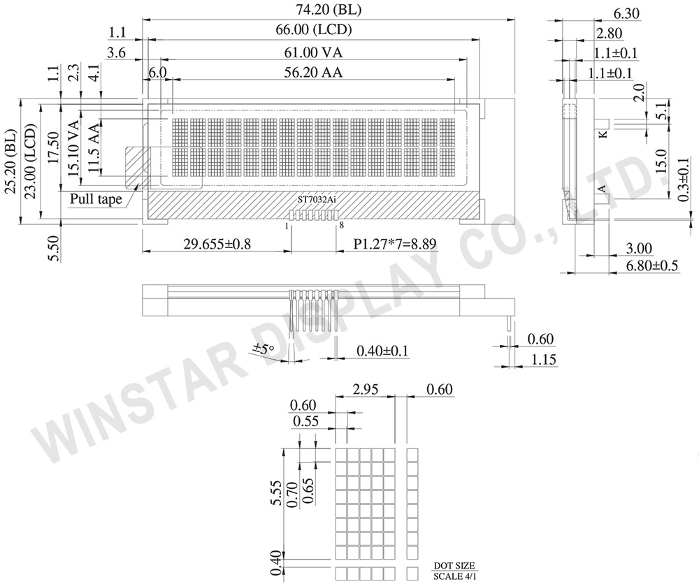
WO1602K 是一款16x2 COG 字符 LCD 显示模块,采用金属引脚设计,搭载 I2C 接口及 ST7032Ai 控制 IC。模块支持 3 V 和 5 V 逻辑电源(VDD),采用 1/16 Duty 驱动方式。
模块外形尺寸为 74.2 x 25.2 x 6.3 mm,可视区域为 61.0 x 15.1 mm,有效显示区域为 56.2 x 11.5 mm。COG(Chip-on-Glass)结构设计使其适用于手持设备、便携式仪器、测试设备、工业控制系统及各类嵌入式应用。
WO1602K 模块工作温度范围为 -20℃ ~ +70℃,存储温度范围为 -30℃ ~ +80℃。WO1602K 也可作为 WO1602G 的替代型号,适用于采用 ST7032Ai 控制 IC 的应用,或在 IC 缺货及交期较长时作为替代方案。
| 项目 | 规格 | 单位 |
|---|---|---|
| 字符数 | 16字 x 2行 | - |
| 模块尺寸 | 74.2 x 25.2 x 6.3 | mm |
| 检视区域 | 61.0 x 15.1 | mm |
| 有效区域 | 56.2 x 11.5 | mm |
| 点大小 | 0.55 x 0.65 | mm |
| 点间距 | 0.60 x 0.70 | mm |
| 字符大小 | 2.95 x 5.55 | mm |
| 字符间距 | 3.55 x 5.95 | mm |
| 驱动方式 | 1/16 Duty , 1/5 Bias | |
| 背光类型 | LED | |
| IC | ST7032Ai | |
| 接口 | I2C | |
| 项目 | 符号 | 最小值 | 标准值 | 最大值 | 单位 |
|---|---|---|---|---|---|
| 工作温度 | TOP | -20 | - | +70 | ℃ |
| 储存温度 | TST | -30 | - | +80 | ℃ |
| 输入电压 | VIN | -0.3 | - | VDD+0.3 | V |
| 电源电压 | VDD-VSS | -0.3 | - | +4.0 | V |
| LCD驱动电压 | VLCD | -0.3 | - | 7.0 | V |
| 项目 | 符号 | 条件 | 最小值 | 标准值 | 最大值 | 单位 |
|---|---|---|---|---|---|---|
| 逻辑电源电压 | VDD-VSS | - | 2.7 | 3.0 | 3.3 | V |
| LCD电源电压 | VLCD | Ta=-20℃ Ta=25℃ Ta=70℃ |
- 4.3 - |
- 4.5 - |
- 4.7 - |
V V V |
| 输入高电压 | VIH | - | 0.7 VDD | - | VDD | V |
| 输入低电压 | VIL | - | VDD | - | 0.3 VDD | V |
| 供电电流 | IDD | - | - | 1.0 | - | mA |
| Pin No. | 符号 | 说明 |
|---|---|---|
| 1 | VG | VG is the LCD driving voltage for segment circuits. VGO is the output of VG regulator. VGS is the feedback of VG regulator. VGI is the VG input of segment circuits. 1.6 ≤ VG < VDD2. |
| 2 | XV0 | XV0 is the LCD driving voltage for common circuits at positive frame. XV0OUT is the output of XV0 regulator. XV0S is the feedback of XV0 regulator. XV0I is the V0 input of common circuits |
| 3 | V0 | V0 is the LCD driving voltage for common circuits at negative frame. V0OUT is the output of V0 regulator. V0S is the feedback of V0 regulator. V0I is the V0 input of common circuits. Be sure that: V0 ≥ VG > VM > VSS ≥ XV0 (under operation). |
| 4 | VDD | Power supply input. |
| 5 | VSS | Ground |
| 6 | SDA | Serial data input |
| 7 | SCL | Serial clock input |
| 8 | RST | Hardware reset input pin. When RSTB is “L”, internal initialization is executed and the internal registers will be initialized. |

通过点击「允许所有 Cookie」,代表您同意在您的设备上存储 Cookie 以增强网站浏览体验、分析网站使用情况并协助我们的营销和网站效能优化工作。您可以在我们的隐私权政策中找到有关于此的更多信息。