


Tela LCD IPS TFT 2,8 polegada 240x320, PCAP
Model No. WF28JTYAJDNF0
►Tamanho: 2,8 polegadas
►Resolução: 240 x 320 pontos
►Direção de exibição: IPS
►Interface: MCU, SPI
►Driver IC:ILI9341
►Placa de controle: Não
►Brilho (cd/m²): 400
►Quadro com furo passante: Não
►Tela de Toque: Com painel de toque capacitivo (PCAP)
Descrição
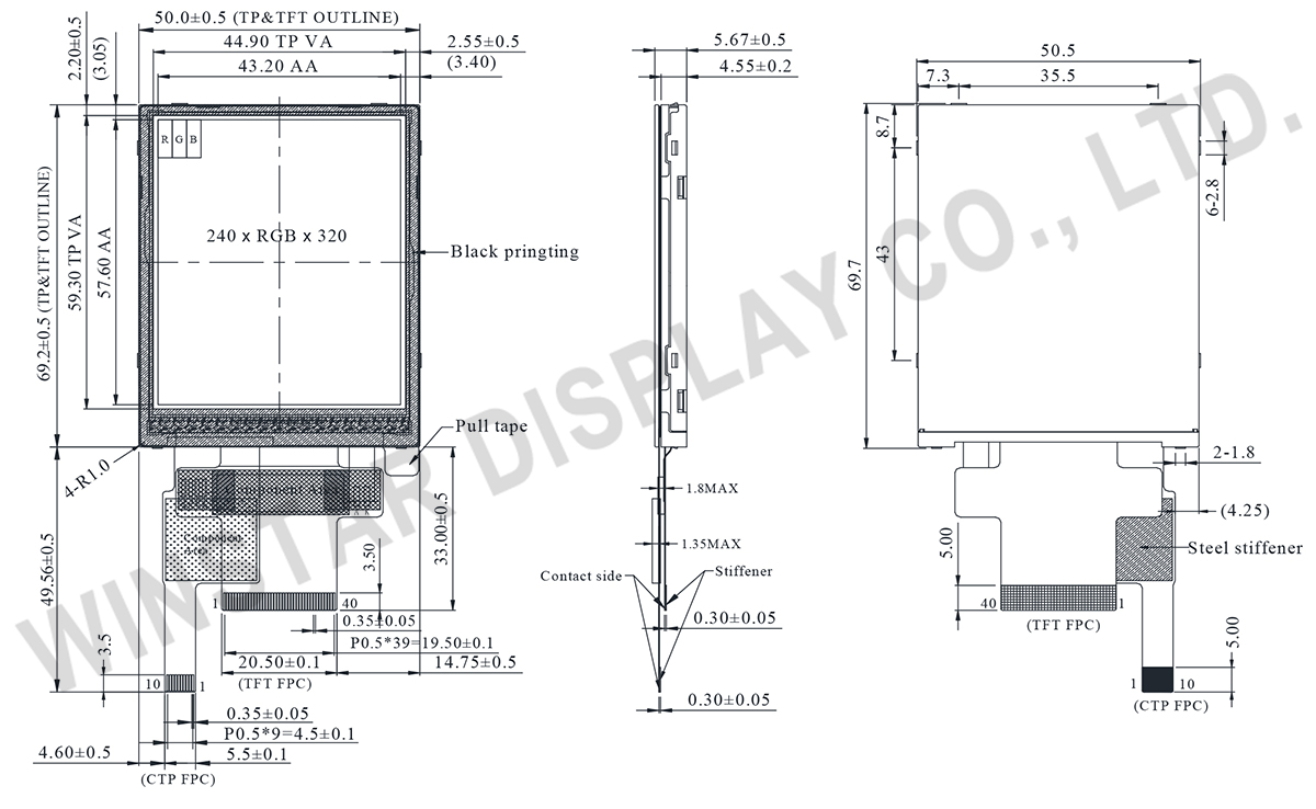
WF28JTYAJDNF0 é um módulo de display TFT de 2,8 polegadas em modo retrato, com uma resolução de 240x320 pixels, uma luminosidade de 400 cd/m2 e uma relação de contraste de 800:1. Este módulo LCD apresenta um painel tátil capacitivo projetado e está equipado com o circuito integrado ILI9341V, suportando interfaces MCU ou SPI. O módulo tem dimensões de 50,5 x 69,7 mm, com uma área ativa de 43,2 x 57,6 mm. A voltagem de alimentação varia de 1,65V a 3,3V. O painel tátil capacitivo projetado é integrado com o circuito integrado FT6336G, suportando a interface I2C e um único ponto de detecção. O módulo pode operar numa faixa de temperatura de -20°C a +70°C, com temperaturas de armazenamento variando de -30°C a +80°C.
WF28JTYAJDNF0 utiliza a tecnologia IPS, proporcionando um amplo ângulo de visão de Esquerda: 80 / Direita: 80 / Cima: 80 / Baixo: 80 graus (valor típico). Os painéis IPS em displays TFT oferecem ângulos de visão mais amplos, reprodução precisa e consistente de cores, qualidade de imagem superior, desempenho preciso de touchscreen e temperatura de cor constante. A versatilidade dos displays TFT-LCD IPS os torna adequados para várias aplicações, incluindo eletrônicos de consumo, displays médicos e painéis de controle industriais.
DRAWING
SPECIFICATIONS
Função do pino de interface
LCM PIN Definition
| NO | Símbolo | Função | I/O | ||||||||||||||||||||||||||||||||||||||||||||
|---|---|---|---|---|---|---|---|---|---|---|---|---|---|---|---|---|---|---|---|---|---|---|---|---|---|---|---|---|---|---|---|---|---|---|---|---|---|---|---|---|---|---|---|---|---|---|---|
| 1 | GND | Ground | P | ||||||||||||||||||||||||||||||||||||||||||||
| 2-6 | NC | No connection | - | ||||||||||||||||||||||||||||||||||||||||||||
| 7 | VCI | High voltage power supply for analog circuit blocks (2.5 ~ 3.3 V) |
P | ||||||||||||||||||||||||||||||||||||||||||||
| 8 | IOVCC | Low voltage power supply for interface logic circuits (2.5 ~ 3.3 V) |
P | ||||||||||||||||||||||||||||||||||||||||||||
| 9 | TE | Tearing effect output pin to synchronize MPU to frame writing, activated by S/W command. When this pin is not activated, this pin is low. If not used, open this pin. |
O | ||||||||||||||||||||||||||||||||||||||||||||
| 10 | CS | Chip select signal. | I | ||||||||||||||||||||||||||||||||||||||||||||
| 11 | D/CX(SCL) | (D/CX): This pin is used to select "Data or Command" in the parallel interface. When DCX = 1, data is selected. When DCX = 0, command is selected. (SCL): This pin is used as the serial interface clock in 3-wire 9-bit/4-wire 8-bit serial data interface. If not used, this pin should be connected to IOVCC or GND. |
I | ||||||||||||||||||||||||||||||||||||||||||||
| 12 | WR(SPI_D/C) | (WRX) - 8080-Ⅰ/8080-Ⅱ system: Serves as a write signal and writes data at the rising edge. (D/CX) - 4-line system: Serves as the selector of command or parameter. Fix to IOVCC level when not in use. |
I | ||||||||||||||||||||||||||||||||||||||||||||
| 13 | RD | 8080-Ⅰ/8080-Ⅱ system (RDX): Serves as a read signal and MCU read data at the rising edge. Fix to IOVCC level when not in use. |
I | ||||||||||||||||||||||||||||||||||||||||||||
| 14-29 | DB0~DB15 | 18-bit parallel bi-directional data bus for MCU system. Fix to GND level when not in use. |
I/O | ||||||||||||||||||||||||||||||||||||||||||||
| 30 | RESET | (RESX)This signal will reset the device and must be applied to properly initialize the chip. Signal is active low. |
I | ||||||||||||||||||||||||||||||||||||||||||||
| 31 | IM0 | Select the MCU interface mode
MPU Parallel interface bus and serial interface select If use RGB Interface must select serial interface. * : Fix this pin at IOVCC or GND. |
I | ||||||||||||||||||||||||||||||||||||||||||||
| 32 | IM1 | ||||||||||||||||||||||||||||||||||||||||||||||
| 33 | IM2 | ||||||||||||||||||||||||||||||||||||||||||||||
| 34 | DB16 | 18-bit parallel bi-directional data bus for MCU system and RGB interface mode Fix to GND level when not in use. |
I/O | ||||||||||||||||||||||||||||||||||||||||||||
| 35 | DB17 | ||||||||||||||||||||||||||||||||||||||||||||||
| 36 | LEDK | Cathode of LED backlight. | P | ||||||||||||||||||||||||||||||||||||||||||||
| 37 | LEDK | Cathode of LED backlight. | P | ||||||||||||||||||||||||||||||||||||||||||||
| 38 | LEDA | Anode of LED backlight. | P | ||||||||||||||||||||||||||||||||||||||||||||
| 39 | SDA | SDA : Serial in/out signal. The data is applied on the rising edge of the SCL signal. If not used, fix this pin at IOVCC or GND. |
I/O | ||||||||||||||||||||||||||||||||||||||||||||
| 40 | NC | Not used, open this pin | N | ||||||||||||||||||||||||||||||||||||||||||||
PCAP PIN Definition
| Pin | Símbolo | Função |
|---|---|---|
| 1 | VSS | Ground for analog circuit |
| 2 | VDDT | Power Supply : +3.3V |
| 3 | SCL | I2C clock input |
| 4 | NC | No connect |
| 5 | SDA | I2C data input and output |
| 6 | NC | No connect |
| 7 | /RST | External Reset, Low is active |
| 8 | NC | No connect |
| 9 | /INT | External interrupt to the host |
| 10 | VSS | Ground for analog circuit |
Especificações Gerais
| Item | Dimensão | Unidade |
|---|---|---|
| Tamanho | 2.8 | inch |
| Matriz de pontos | 240 x RGB x 320(TFT) | dots |
| Dimensão do módulo | 50.5(W) x 69.7(H) x5.67(D) | mm |
| Área ativa (AA) | 43.2 x 57.6 | mm |
| Distância entre pontos | 0.18 x 0.18 | mm |
| Tipo LCD | TFT, Preto, Transmissivo | |
| TFT IC do controlador | ILI9341V ou equivalente | |
| TFT Interface | MCU/SPI | |
| Direção de exibição | 80/80/80/80 | |
| Relação de aspecto | 3:4 | |
| Tipo de luz de fundo | LED, Branco | |
| PCAP IC | FT6336G ou equivalente | |
| PCAP Interface | I2C | |
| PCAP FW | 0x11 | |
| Painel de toque | painel de toque capacitivo | |
| Superfície | Reflexo | |
Classificações Máximas Absolutas
| Item | Símbolo | Valor Min | Valor Típico | Valor Máximo | Unidade |
|---|---|---|---|---|---|
| Temperatura de operação | TOP | -20 | - | +70 | ℃ |
| Temperatura de armazenamento | TST | -30 | - | +80 | ℃ |
Características Eletrônicas
Operating conditions
| Item | Símbolo | Condição | Valor Min | Valor Típico | Valor Máximo | Unidade |
|---|---|---|---|---|---|---|
| Supply Voltage for digital | IOVCC | - | 1.65 | - | 3.3 | V |
| Supply Voltage for analog | VCI | - | 2.5 | - | 3.3 | V |
| Supply Voltage For Touch Logic | VDDT | - | 3.0 | 3.3 | 3.6 | V |
| Power Supply for Current | ICC | IOVCC=VCI =VCC=3.0V |
- | 13 | 20 | mA |
LED driving conditions
| Parameter | Símbolo | Valor Min | Valor Típico | Valor Máximo | Unidade |
|---|---|---|---|---|---|
| LED current | - | - | 80 | - | mA |
| LED voltage | LEDA | 8.1 | 9.3 | 10.5 | V |
| LED Life Time | - | 50000 | - | - | Hr |
