
 - WF28JTYAJDNF0")
 - WF28JTYAJDNF0")
2.8" IPS 240x320 Display LCD TFT IPS(PCAP)
Modello numero WF28JTYAJDNF0
►Dimensione : 2.8 pollici
►Risoluzione : 240 x 320 punti
►Direzione di visione : IPS
►Interfaccia : MCU, SPI
►Driver IC:ILI9341
►Scheda di controllo: No
►Luminosità (cd/m²): 400
►Cornice di fissaggio: No
►Touch Screen: con schermoo touch capacitivo (PCAP)
Descrizione
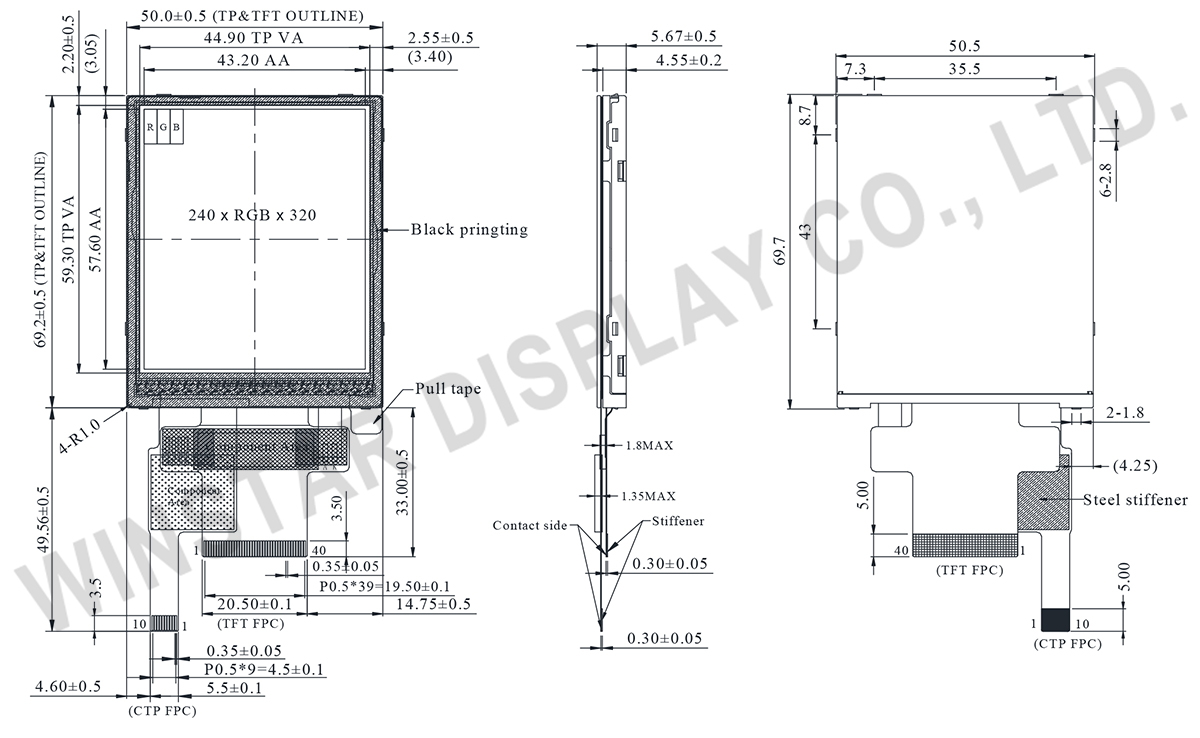
WF28JTYAJDNF0 è un modulo display TFT da 2,8 pollici in modalità ritratto con una risoluzione di 240x320 pixel, una luminosità di 400 cd/m2 e un rapporto di contrasto di 800:1. Questo modulo LCD presenta un pannello tattile capacitivo proiettato ed è dotato del circuito integrato ILI9341V, che supporta le interfacce MCU o SPI. Il modulo ha dimensioni di 50,5 x 69,7 mm, con un'area attiva di 43,2 x 57,6 mm. La tensione di alimentazione varia da 1.65V a 3.3V. Il pannello tattile capacitivo proiettato è integrato con il circuito integrato FT6336G, che supporta l'interfaccia I2C e un singolo punto di rilevamento. Il modulo può operare in un intervallo di temperature compreso tra -20°C e +70°C; le temperature di conservazione vanno da -30°C a +80°C.
WF28JTYAJDNF0 utilizza la tecnologia IPS, offrendo un'ampia angolazione di visione di Sinistra: 80 / Destra: 80 / Su: 80 / Giù: 80 gradi (valore tipico). I pannelli IPS nei display TFT offrono angoli di visione più ampi, riproduzione accurata e coerente dei colori, qualità dell'immagine superiore, prestazioni precise del touchscreen e temperatura del colore uniforme. La versatilità dei display TFT-LCD IPS li rende adatti a varie applicazioni, tra cui dispositivi di elettronica di consumo, display medici e pannelli di controllo industriali.
DISEGNO
SPECIFICHE TECNICHE
Funzione dei Pin di Interfaccia
LCM PIN Definition
| NO | Simbolo | Funzione | I/O | ||||||||||||||||||||||||||||||||||||||||||||
|---|---|---|---|---|---|---|---|---|---|---|---|---|---|---|---|---|---|---|---|---|---|---|---|---|---|---|---|---|---|---|---|---|---|---|---|---|---|---|---|---|---|---|---|---|---|---|---|
| 1 | GND | Ground | P | ||||||||||||||||||||||||||||||||||||||||||||
| 2-6 | NC | No connection | - | ||||||||||||||||||||||||||||||||||||||||||||
| 7 | VCI | High voltage power supply for analog circuit blocks (2.5 ~ 3.3 V) |
P | ||||||||||||||||||||||||||||||||||||||||||||
| 8 | IOVCC | Low voltage power supply for interface logic circuits (2.5 ~ 3.3 V) |
P | ||||||||||||||||||||||||||||||||||||||||||||
| 9 | TE | Tearing effect output pin to synchronize MPU to frame writing, activated by S/W command. When this pin is not activated, this pin is low. If not used, open this pin. |
O | ||||||||||||||||||||||||||||||||||||||||||||
| 10 | CS | Chip select signal. | I | ||||||||||||||||||||||||||||||||||||||||||||
| 11 | D/CX(SCL) | (D/CX): This pin is used to select "Data or Command" in the parallel interface. When DCX = 1, data is selected. When DCX = 0, command is selected. (SCL): This pin is used as the serial interface clock in 3-wire 9-bit/4-wire 8-bit serial data interface. If not used, this pin should be connected to IOVCC or GND. |
I | ||||||||||||||||||||||||||||||||||||||||||||
| 12 | WR(SPI_D/C) | (WRX) - 8080-Ⅰ/8080-Ⅱ system: Serves as a write signal and writes data at the rising edge. (D/CX) - 4-line system: Serves as the selector of command or parameter. Fix to IOVCC level when not in use. |
I | ||||||||||||||||||||||||||||||||||||||||||||
| 13 | RD | 8080-Ⅰ/8080-Ⅱ system (RDX): Serves as a read signal and MCU read data at the rising edge. Fix to IOVCC level when not in use. |
I | ||||||||||||||||||||||||||||||||||||||||||||
| 14-29 | DB0~DB15 | 18-bit parallel bi-directional data bus for MCU system. Fix to GND level when not in use. |
I/O | ||||||||||||||||||||||||||||||||||||||||||||
| 30 | RESET | (RESX)This signal will reset the device and must be applied to properly initialize the chip. Signal is active low. |
I | ||||||||||||||||||||||||||||||||||||||||||||
| 31 | IM0 | Select the MCU interface mode
MPU Parallel interface bus and serial interface select If use RGB Interface must select serial interface. * : Fix this pin at IOVCC or GND. |
I | ||||||||||||||||||||||||||||||||||||||||||||
| 32 | IM1 | ||||||||||||||||||||||||||||||||||||||||||||||
| 33 | IM2 | ||||||||||||||||||||||||||||||||||||||||||||||
| 34 | DB16 | 18-bit parallel bi-directional data bus for MCU system and RGB interface mode Fix to GND level when not in use. |
I/O | ||||||||||||||||||||||||||||||||||||||||||||
| 35 | DB17 | ||||||||||||||||||||||||||||||||||||||||||||||
| 36 | LEDK | Cathode of LED backlight. | P | ||||||||||||||||||||||||||||||||||||||||||||
| 37 | LEDK | Cathode of LED backlight. | P | ||||||||||||||||||||||||||||||||||||||||||||
| 38 | LEDA | Anode of LED backlight. | P | ||||||||||||||||||||||||||||||||||||||||||||
| 39 | SDA | SDA : Serial in/out signal. The data is applied on the rising edge of the SCL signal. If not used, fix this pin at IOVCC or GND. |
I/O | ||||||||||||||||||||||||||||||||||||||||||||
| 40 | NC | Not used, open this pin | N | ||||||||||||||||||||||||||||||||||||||||||||
PCAP PIN Definition
| Pin | Simbolo | Funzione |
|---|---|---|
| 1 | VSS | Ground for analog circuit |
| 2 | VDDT | Power Supply : +3.3V |
| 3 | SCL | I2C clock input |
| 4 | NC | No connect |
| 5 | SDA | I2C data input and output |
| 6 | NC | No connect |
| 7 | /RST | External Reset, Low is active |
| 8 | NC | No connect |
| 9 | /INT | External interrupt to the host |
| 10 | VSS | Ground for analog circuit |
Specifiche generali
| Articolo | Dimensioni | Unità |
|---|---|---|
| Dimensione (Diagonale) | 2.8 | pollici |
| A matrice di punti (Risoluzione) | 240 x RGB x 320(TFT) | punti |
| Dimensione del modulo | 50.5(W) x 69.7(H) x5.67(D) | mm |
| Area attiva (AA) | 43.2 x 57.6 | mm |
| Passo del Dot | 0.18 x 0.18 | mm |
| Tipo LCD | TFT, Nero, Trasmissivo | |
| TFT Driver IC | ILI9341V o equivalente | |
| TFT Interfaccia | MCU/SPI | |
| Direzione di visione | 80/80/80/80 | |
| Proporzioni dell’area visiva (ratio) | 3:4 | |
| Tipo di backlight | LED, Bianco | |
| PCAP IC | FT6336G o equivalente | |
| PCAP Interfaccia | I2C | |
| PCAP FW | 0x11 | |
| Touch Screen | con pannello touch capacitivo | |
| Superficie | Bagliore (Glare) | |
Valori massimi assoluti
| Articolo | Simbolo | Valore Min | Valore tipico | Valore massimo | Unità |
|---|---|---|---|---|---|
| Temperatura di lavoro | TOP | -20 | - | +70 | ℃ |
| Temperatura di stock | TST | -30 | - | +80 | ℃ |
Caratteristiche elettriche
Operating conditions
| Articolo | Simbolo | Condizione | Valore Min | Valore tipico | Valore massimo | Unità |
|---|---|---|---|---|---|---|
| Supply Voltage for digital | IOVCC | - | 1.65 | - | 3.3 | V |
| Supply Voltage for analog | VCI | - | 2.5 | - | 3.3 | V |
| Supply Voltage For Touch Logic | VDDT | - | 3.0 | 3.3 | 3.6 | V |
| Power Supply for Current | ICC | IOVCC=VCI =VCC=3.0V |
- | 13 | 20 | mA |
LED driving conditions
| Parameter | Simbolo | Valore Min | Valore tipico | Valore massimo | Unità |
|---|---|---|---|---|---|
| LED current | - | - | 80 | - | mA |
| LED voltage | LEDA | 8.1 | 9.3 | 10.5 | V |
| LED Life Time | - | 50000 | - | - | Hr |
