


2,8 Zoll TFT 240x320 IPS Bildschirm Touchscreen
Modellnummer WF28JTYAJDNF0
►Größe: 2,8 Zoll
►Auflösung: 240 x 320 Punkten
►Betrachtungsrichtung: IPS
►Schnittstelle: MCU, SPI
►Treiber IC:ILI9341
►Steuerplatine: Nein
►Helligkeit (cd/m²): 400
►Durchsteckrahmen: Nein
►Touchscreen: Kapazitiver Touchscreen (PCAP/PCT)
Beschreibung
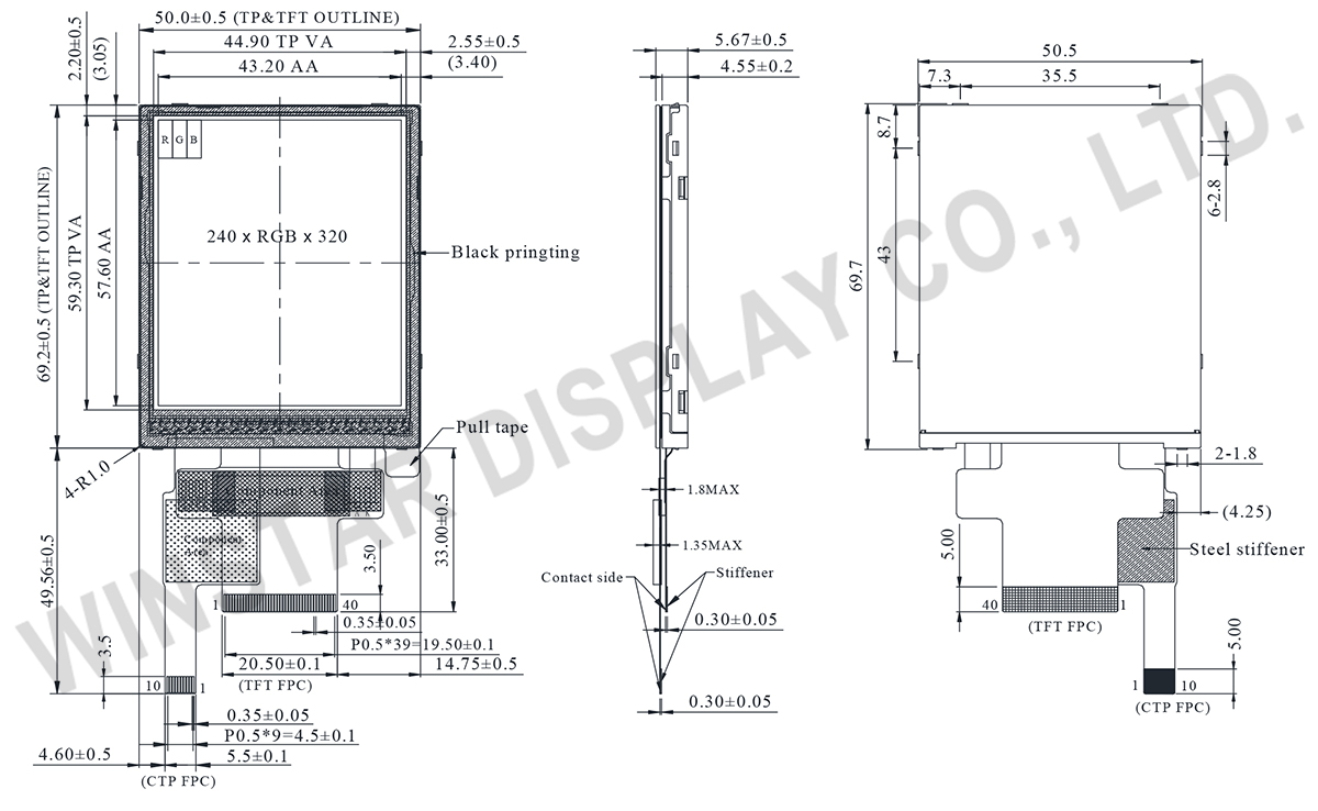
WF28JTYAJDNF0 ist ein 2,8-Zoll-TFT-Display-Modul im Hochformat mit einer Auflösung von 240x320 Pixeln, einer Helligkeit von 400 cd/m2 und einem Kontrastverhältnis von 800:1. Dieses LCD-Modul verfügt über ein projiziertes kapazitives Touchpanel und ist mit dem ILI9341V-IC ausgestattet, das MCU- oder SPI-Schnittstellen unterstützt. Das Modul hat Abmessungen von 50,5 x 69,7 mm und eine aktive Fläche von 43,2 x 57,6 mm. Die Versorgungsspannung liegt zwischen 1,65V und 3,3V. Das projizierte kapazitive Touchpanel ist mit dem FT6336G-IC integriert, das die I2C-Schnittstelle und einen einzelnen Erfassungspunkt unterstützt. Das Modul kann in einem Temperaturbereich von -20°C bis +70°C betrieben werden, und die Lagertemperaturen liegen zwischen -30°C und +80°C.
WF28JTYAJDNF0 verwendet die IPS-Technologie und bietet einen weiten Betrachtungswinkel von Links: 80 / Rechts: 80 / Oben: 80 / Unten: 80 Grad (typischer Wert). IPS-Panels in TFT-Displays bieten breitere Betrachtungswinkel, genaue und konsistente Farbwiedergabe, überlegene Bildqualität, präzise Touchscreen-Performance und eine konstante Farbtemperatur. Die Vielseitigkeit von IPS TFT-LCD-Displays macht sie für verschiedene Anwendungen geeignet, darunter Unterhaltungselektronik, medizinische Displays und industrielle Bedienfelder.
Zeichnung
Technische Daten
Schnittstelle Pin-Funktion
LCM PIN Definition
| NO | Symbol | Funktion | I/O | ||||||||||||||||||||||||||||||||||||||||||||
|---|---|---|---|---|---|---|---|---|---|---|---|---|---|---|---|---|---|---|---|---|---|---|---|---|---|---|---|---|---|---|---|---|---|---|---|---|---|---|---|---|---|---|---|---|---|---|---|
| 1 | GND | Ground | P | ||||||||||||||||||||||||||||||||||||||||||||
| 2-6 | NC | No connection | - | ||||||||||||||||||||||||||||||||||||||||||||
| 7 | VCI | High voltage power supply for analog circuit blocks (2.5 ~ 3.3 V) |
P | ||||||||||||||||||||||||||||||||||||||||||||
| 8 | IOVCC | Low voltage power supply for interface logic circuits (2.5 ~ 3.3 V) |
P | ||||||||||||||||||||||||||||||||||||||||||||
| 9 | TE | Tearing effect output pin to synchronize MPU to frame writing, activated by S/W command. When this pin is not activated, this pin is low. If not used, open this pin. |
O | ||||||||||||||||||||||||||||||||||||||||||||
| 10 | CS | Chip select signal. | I | ||||||||||||||||||||||||||||||||||||||||||||
| 11 | D/CX(SCL) | (D/CX): This pin is used to select "Data or Command" in the parallel interface. When DCX = 1, data is selected. When DCX = 0, command is selected. (SCL): This pin is used as the serial interface clock in 3-wire 9-bit/4-wire 8-bit serial data interface. If not used, this pin should be connected to IOVCC or GND. |
I | ||||||||||||||||||||||||||||||||||||||||||||
| 12 | WR(SPI_D/C) | (WRX) - 8080-Ⅰ/8080-Ⅱ system: Serves as a write signal and writes data at the rising edge. (D/CX) - 4-line system: Serves as the selector of command or parameter. Fix to IOVCC level when not in use. |
I | ||||||||||||||||||||||||||||||||||||||||||||
| 13 | RD | 8080-Ⅰ/8080-Ⅱ system (RDX): Serves as a read signal and MCU read data at the rising edge. Fix to IOVCC level when not in use. |
I | ||||||||||||||||||||||||||||||||||||||||||||
| 14-29 | DB0~DB15 | 18-bit parallel bi-directional data bus for MCU system. Fix to GND level when not in use. |
I/O | ||||||||||||||||||||||||||||||||||||||||||||
| 30 | RESET | (RESX)This signal will reset the device and must be applied to properly initialize the chip. Signal is active low. |
I | ||||||||||||||||||||||||||||||||||||||||||||
| 31 | IM0 | Select the MCU interface mode
MPU Parallel interface bus and serial interface select If use RGB Interface must select serial interface. * : Fix this pin at IOVCC or GND. |
I | ||||||||||||||||||||||||||||||||||||||||||||
| 32 | IM1 | ||||||||||||||||||||||||||||||||||||||||||||||
| 33 | IM2 | ||||||||||||||||||||||||||||||||||||||||||||||
| 34 | DB16 | 18-bit parallel bi-directional data bus for MCU system and RGB interface mode Fix to GND level when not in use. |
I/O | ||||||||||||||||||||||||||||||||||||||||||||
| 35 | DB17 | ||||||||||||||||||||||||||||||||||||||||||||||
| 36 | LEDK | Cathode of LED backlight. | P | ||||||||||||||||||||||||||||||||||||||||||||
| 37 | LEDK | Cathode of LED backlight. | P | ||||||||||||||||||||||||||||||||||||||||||||
| 38 | LEDA | Anode of LED backlight. | P | ||||||||||||||||||||||||||||||||||||||||||||
| 39 | SDA | SDA : Serial in/out signal. The data is applied on the rising edge of the SCL signal. If not used, fix this pin at IOVCC or GND. |
I/O | ||||||||||||||||||||||||||||||||||||||||||||
| 40 | NC | Not used, open this pin | N | ||||||||||||||||||||||||||||||||||||||||||||
PCAP PIN Definition
| Pin | Symbol | Funktion |
|---|---|---|
| 1 | VSS | Ground for analog circuit |
| 2 | VDDT | Power Supply : +3.3V |
| 3 | SCL | I2C clock input |
| 4 | NC | No connect |
| 5 | SDA | I2C data input and output |
| 6 | NC | No connect |
| 7 | /RST | External Reset, Low is active |
| 8 | NC | No connect |
| 9 | /INT | External interrupt to the host |
| 10 | VSS | Ground for analog circuit |
Allgemeine Spezifikationen
| Artikel | Ausmaß | Einheit |
|---|---|---|
| Größe (Diagonale) | 2.8 | Zoll |
| Punktmatrix (Auflösung) | 240 x RGB x 320(TFT) | Punkte |
| Abmaße der modul | 50.5(W) x 69.7(H) x5.67(D) | mm |
| Aktiver Bereich (AA) | 43.2 x 57.6 | mm |
| Punktabstand | 0.18 x 0.18 | mm |
| LCD-Typ | TFT, Schwarz, Transmissiv | |
| TFT Treiber IC | ILI9341V oder gleichwertig | |
| TFT Schnittstelle | MCU/SPI | |
| Blickwinkel | 80/80/80/80 | |
| Seitenverhältnis | 3:4 | |
| Backlight-Typ | LED, Weiß | |
| PCAP IC | FT6336G oder gleichwertig | |
| PCAP Interface | I2C | |
| PCAP FW | 0x11 | |
| Touchscreen | projiziert kapazitives Touch-Panel | |
| Oberfläche | Glanz | |
absolute Grenzwerte
| Artikel | Symbol | Mindestwert | typischer Wert | Max | Einheit |
|---|---|---|---|---|---|
| Operating Temperature | TOP | -20 | - | +70 | ℃ |
| Storage Temperature | TST | -30 | - | +80 | ℃ |
Electrical Characteristics
Operating conditions
| Artikel | Symbol | Bedingung | Mindestwert | typischer Wert | Maximalwert | Einheit |
|---|---|---|---|---|---|---|
| Supply Voltage for digital | IOVCC | - | 1.65 | - | 3.3 | V |
| Supply Voltage for analog | VCI | - | 2.5 | - | 3.3 | V |
| Supply Voltage For Touch Logic | VDDT | - | 3.0 | 3.3 | 3.6 | V |
| Power Supply for Current | ICC | IOVCC=VCI =VCC=3.0V |
- | 13 | 20 | mA |
LED driving conditions
| Parameter | Symbol | Mindestwert | typischer Wert | Maximalwert | Einheit |
|---|---|---|---|---|---|
| LED current | - | - | 80 | - | mA |
| LED voltage | LEDA | 8.1 | 9.3 | 10.5 | V |
| LED Life Time | - | 50000 | - | - | Hr |
