Tela LCD IPS TFT 2,8 polegada 240x320, ILI9341
Model No. WF28JTYAJDNN0
►Tamanho: 2,8 polegadas
►Resolução: 240 x 320 pontos
►Direção de exibição: IPS
►Interface: MCU, SPI
►Driver IC:ILI9341
►Placa de controle: Não
►Brilho (cd/m²): 500
►Quadro com furo passante: Não
►Tela de Toque: Não
Descrição
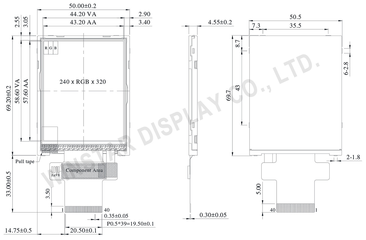
WF28JTYAJDNN0 é um módulo de tela LCD TFT IPS de 2,8 polegadas com um ângulo de visão mais amplo, uma resolução de 240x320 pixels e uma proporção de aspecto de 3:4. O módulo WF28JTYAJDNN0 é projetado em modo retrato como um LCD TFT IPS, incorporando o controlador IC ILI9341. Ele suporta interfaces MCU de 8 bits/16 bits ou SPI, proporcionando uma razão de contraste típica de 800:1. O brilho do WF28JTYAJDNN0 é de 500 nits (valor típico).
A voltagem de alimentação para a lógica de interface (IOVCC) do modelo WF28J varia de 1,65V a 3,3V, enquanto a alimentação para o circuito analógico é de 2,5V a 3,3V. É um tipo de LCD normalmente preto, transmissivo, com uma superfície de vidro anti-reflexo. A faixa de temperatura de operação vai de -20°C a +70°C, e as temperaturas de armazenamento variam de -30°C a +80°C.
Este TFT IPS de 2,8 polegadas oferece um ângulo de visão mais amplo em comparação com o TFT TN, com ângulos de Esquerda: 80 / Direita: 80 / Cima: 80 / Baixo: 80 graus (valor típico). Painéis IPS em telas TFT oferecem ângulos de visão mais amplos, reprodução de cor precisa e consistente, qualidade de imagem superior, desempenho preciso de tela sensível ao toque e temperatura de cor consistente. A versatilidade dos displays TFT-LCD IPS os torna adequados para várias aplicações, incluindo eletrônicos de consumo, telas médicas e painéis de controle industriais.
DRAWING
SPECIFICATIONS
Função do pino de interface
LCM PIN Definition
NO | Símbolo | Função | I/O | ||||||||||||||||||||||||||||||||||||||||||||
---|---|---|---|---|---|---|---|---|---|---|---|---|---|---|---|---|---|---|---|---|---|---|---|---|---|---|---|---|---|---|---|---|---|---|---|---|---|---|---|---|---|---|---|---|---|---|---|
1 | GND | Ground | P | ||||||||||||||||||||||||||||||||||||||||||||
2-6 | NC | No connection | - | ||||||||||||||||||||||||||||||||||||||||||||
7 | VCI | High voltage power supply for analog circuit blocks (2.5 ~ 3.3 V) |
P | ||||||||||||||||||||||||||||||||||||||||||||
8 | IOVCC | Low voltage power supply for interface logic circuits (2.5 ~ 3.3 V) |
P | ||||||||||||||||||||||||||||||||||||||||||||
9 | TE | Tearing effect output pin to synchronize MPU to frame writing, activated by S/W command. When this pin is not activated, this pin is low. If not used, open this pin. |
O | ||||||||||||||||||||||||||||||||||||||||||||
10 | CS | Chip select signal. | I | ||||||||||||||||||||||||||||||||||||||||||||
11 | D/CX(SCL) | (D/CX): This pin is used to select “Data or Command” in the parallel interface. When DCX = 1, data is selected. When DCX = 0, command is selected. (SCL): This pin is used as the serial interface clock in 3-wire 9-bit/4-wire 8-bit serial data interface. If not used, this pin should be connected to IOVCC or GND. |
I | ||||||||||||||||||||||||||||||||||||||||||||
12 | WR(SPI_D/C) | (WRX) - 8080-Ⅰ/8080-Ⅱ system: Serves as a write signal and writes data at the rising edge. (D/CX) - 4-line system: Serves as the selector of command or parameter. Fix to IOVCC level when not in use. |
I | ||||||||||||||||||||||||||||||||||||||||||||
13 | RD | 8080-Ⅰ/8080-Ⅱ system (RDX): Serves as a read signal and MCU read data at the rising edge. Fix to IOVCC level when not in use. |
I | ||||||||||||||||||||||||||||||||||||||||||||
14-29 | DB0~DB15 | 18-bit parallel bi-directional data bus for MCU system. Fix to GND level when not in use. |
I/O | ||||||||||||||||||||||||||||||||||||||||||||
30 | RESET | (RESX)This signal will reset the device and must be applied to properly initialize the chip. Signal is active low. |
I | ||||||||||||||||||||||||||||||||||||||||||||
31 | IM0 | Select the MCU interface mode
MPU Parallel interface bus and serial interface select If use RGB Interface must select serial interface. * : Fix this pin at IOVCC or GND. |
I | ||||||||||||||||||||||||||||||||||||||||||||
32 | IM1 | ||||||||||||||||||||||||||||||||||||||||||||||
33 | IM2 | ||||||||||||||||||||||||||||||||||||||||||||||
34 | DB16 | 18-bit parallel bi-directional data bus for MCU system and RGB interface mode Fix to GND level when not in use. |
I/O | ||||||||||||||||||||||||||||||||||||||||||||
35 | DB17 | ||||||||||||||||||||||||||||||||||||||||||||||
36 | LEDK | Cathode of LED backlight. | P | ||||||||||||||||||||||||||||||||||||||||||||
37 | LEDK | Cathode of LED backlight. | P | ||||||||||||||||||||||||||||||||||||||||||||
38 | LEDA | Anode of LED backlight. | P | ||||||||||||||||||||||||||||||||||||||||||||
39 | SDA | SDA : Serial in/out signal. The data is applied on the rising edge of the SCL signal. If not used, fix this pin at IOVCC or GND. |
I/O | ||||||||||||||||||||||||||||||||||||||||||||
40 | NC | Not used, open this pin | N |
Especificações Gerais
Item | Dimensão | Unidade |
---|---|---|
Tamanho | 2,8 | polegadas |
Matriz de pontos | 240 x RGB x 320(TFT) | pontos |
Dimensão do módulo | 50.5(W) x 69.7(H) x 4.55(D) | mm |
Área ativa | 43.2 x 57.6 | mm |
Distância entre pontos | 0.18 x 0.18 | mm |
Tipo LCD | TFT, Preto, Transmissivo | |
TFT IC do controlador | ILI9341V ou equivalente | |
TFT Interface | MCU/SPI | |
Direção de exibição | 80/80/80/80 | |
Relação de aspecto | 3:4 | |
Tipo de luz de fundo | LED, Branco | |
Painel de toque | Sem painel de toque | |
Superfície | Reflexo |
Classificações Máximas Absolutas
Item | Símbolo | Valor Min | Valor Típico | Valor Máximo | Unidade |
---|---|---|---|---|---|
Temperatura de operação | TOP | -20 | - | +70 | ℃ |
Temperatura de armazenamento | TST | -30 | - | +80 | ℃ |
Características Eletrônicas
Item | Symbol | Condição | Valor Min | Valor Típico | Valor Máximo | Unidade |
---|---|---|---|---|---|---|
Supply Voltage for digital | IOVCC | - | 1.65 | - | 3.3 | V |
Supply Voltage for analog | VCI | - | 2.5 | - | 3.3 | V |
Power Supply for Current | ICC | IOVCC=VCI =VCC=3.0V |
- | 13 | 20 | mA |