
我们重视您的隐私
通过点击「允许所有 Cookie」,代表您同意在您的设备上存储 Cookie 以增强网站浏览体验、分析网站使用情况并协助我们的营销和网站效能优化工作。您可以在我们的隐私权政策中找到有关于此的更多信息。


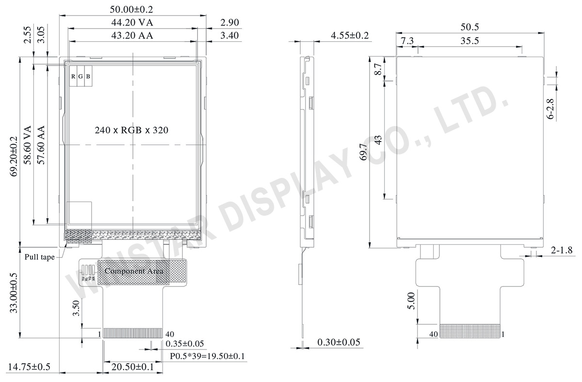
WF28JTYAJDNN0是一款采用IPS面板的2.8吋TFT液晶显示器模块,分辨率240x320像素,屏幕长宽比3:4 为直屏模式IPS模块。模块内建 ILI9341 驱动 IC,支持MCU 8-bit/16-bit与SPI接口,对比度800:1 (典型值),亮度为500 nits(典型值)。WF28J模块的驱动接口电路的电压范围从1.65V~3.3V,仿真供电电压范围从2.5V~3.3V,平常黑/透射式LCD,亮面玻璃。WF28JTYAJDNN0采用IPS面板技术,具广视角范围,左: 80 / 右: 80 / 上: 80 / 下: 80 度,面板视角宽度广,色彩鲜明、具有饱和自然的优质画面。此款模块的工作温度是-20℃ 至 +70℃,储存温度是 -30℃ 至 +80℃。如果客户产品应用需要使用高亮TFT,可另选WF28JSYAJDNN0型号,其模块亮度为1000 nits (典型值)。WF28J系列同时也有电阻式与电容式触控面板可供选择。
| 项目 | 规格 | 单位 |
|---|---|---|
| 尺寸 (对角线) | 2.8 | 寸 |
| 分辨率 | 240 x RGB x 320(TFT) | dots |
| 模块尺寸 | 50.5(W) x 69.7(H) x 4.55(D) | mm |
| 有效区域 | 43.2 x 57.6 | mm |
| 点间距 | 0.18 x 0.18 | mm |
| LCD类型 | TFT全透 | |
| TFT控制器IC | ILI9341V 或兼容IC | |
| TFT接口 | MCU/SPI | |
| 视角 | 80/80/80/80 | |
| 长宽比 | 3:4 | |
| 背光类型 | LED ,平常白 | |
| 触控面板 | 无触控面板 | |
| 表面 | 亮面 | |
| 项目 | 符号 | 最小值 | 典型值 | 最大值 | 单位 |
|---|---|---|---|---|---|
| 工作温度 | TOP | -20 | - | +70 | ℃ |
| 储存温度 | TST | -30 | - | +80 | ℃ |
| 项目 | 符号 | 条件 | 最小值 | 典型值 | 最大值 | 单位 |
|---|---|---|---|---|---|---|
| 数字电源电压 | IOVCC | - | 1.65 | - | 3.3 | V |
| 模拟电源电压 | VCI | - | 2.5 | - | 3.3 | V |
| 电源电流 | ICC | IOVCC=VCI =VCC=3.0V |
- | 13 | 20 | mA |
| 参数 | 符号 | 最小值 | 典型值 | 最大值 | 单位 |
|---|---|---|---|---|---|
| LED电流 | — | — | 80 | — | mA |
| LED电压 | LEDA | 8.1 | 9.3 | 10.5 | V |
| LED使用寿命 | — | 50000 | — | — | Hr |
| NO | 符号 | 功能 | I/O | ||||||||||||||||||||||||||||||||||||||||||||
|---|---|---|---|---|---|---|---|---|---|---|---|---|---|---|---|---|---|---|---|---|---|---|---|---|---|---|---|---|---|---|---|---|---|---|---|---|---|---|---|---|---|---|---|---|---|---|---|
| 1 | GND | Ground | P | ||||||||||||||||||||||||||||||||||||||||||||
| 2-6 | NC | No connection | - | ||||||||||||||||||||||||||||||||||||||||||||
| 7 | VCI | High voltage power supply for analog circuit blocks (2.5 ~ 3.3 V) |
P | ||||||||||||||||||||||||||||||||||||||||||||
| 8 | IOVCC | Low voltage power supply for interface logic circuits (2.5 ~ 3.3 V) |
P | ||||||||||||||||||||||||||||||||||||||||||||
| 9 | TE | Tearing effect output pin to synchronize MPU to frame writing, activated by S/W command. When this pin is not activated, this pin is low. If not used, open this pin. |
O | ||||||||||||||||||||||||||||||||||||||||||||
| 10 | CS | Chip select signal. | I | ||||||||||||||||||||||||||||||||||||||||||||
| 11 | D/CX(SCL) | (D/CX): This pin is used to select “Data or Command” in the parallel interface. When DCX = 1, data is selected. When DCX = 0, command is selected. (SCL): This pin is used as the serial interface clock in 3-wire 9-bit/4-wire 8-bit serial data interface. If not used, this pin should be connected to IOVCC or GND. |
I | ||||||||||||||||||||||||||||||||||||||||||||
| 12 | WR(SPI_D/C) | (WRX) - 8080-Ⅰ/8080-Ⅱ system: Serves as a write signal and writes data at the rising edge. (D/CX) - 4-line system: Serves as the selector of command or parameter. Fix to IOVCC level when not in use. |
I | ||||||||||||||||||||||||||||||||||||||||||||
| 13 | RD | 8080-Ⅰ/8080-Ⅱ system (RDX): Serves as a read signal and MCU read data at the rising edge. Fix to IOVCC level when not in use. |
I | ||||||||||||||||||||||||||||||||||||||||||||
| 14-29 | DB0~DB15 | 18-bit parallel bi-directional data bus for MCU system. Fix to GND level when not in use. |
I/O | ||||||||||||||||||||||||||||||||||||||||||||
| 30 | RESET | (RESX)This signal will reset the device and must be applied to properly initialize the chip. Signal is active low. |
I | ||||||||||||||||||||||||||||||||||||||||||||
| 31 | IM0 | Select the MCU interface mode
MPU Parallel interface bus and serial interface select If use RGB Interface must select serial interface. * : Fix this pin at IOVCC or GND. |
I | ||||||||||||||||||||||||||||||||||||||||||||
| 32 | IM1 | ||||||||||||||||||||||||||||||||||||||||||||||
| 33 | IM2 | ||||||||||||||||||||||||||||||||||||||||||||||
| 34 | DB16 | 18-bit parallel bi-directional data bus for MCU system and RGB interface mode Fix to GND level when not in use. |
I/O | ||||||||||||||||||||||||||||||||||||||||||||
| 35 | DB17 | ||||||||||||||||||||||||||||||||||||||||||||||
| 36 | LEDK | Cathode of LED backlight. | P | ||||||||||||||||||||||||||||||||||||||||||||
| 37 | LEDK | Cathode of LED backlight. | P | ||||||||||||||||||||||||||||||||||||||||||||
| 38 | LEDA | Anode of LED backlight. | P | ||||||||||||||||||||||||||||||||||||||||||||
| 39 | SDA | SDA : Serial in/out signal. The data is applied on the rising edge of the SCL signal. If not used, fix this pin at IOVCC or GND. |
I/O | ||||||||||||||||||||||||||||||||||||||||||||
| 40 | NC | Not used, open this pin | N | ||||||||||||||||||||||||||||||||||||||||||||

通过点击「允许所有 Cookie」,代表您同意在您的设备上存储 Cookie 以增强网站浏览体验、分析网站使用情况并协助我们的营销和网站效能优化工作。您可以在我们的隐私权政策中找到有关于此的更多信息。