 - WF24LSYAJDNN0")


 - WL0F00101000JGDAESA02")
 TFT LCD (Raspberry Pi用) 10.1 インチ ディスプレイ - WF101LSYFPLHGV")
私たちはあなたのプライバシーを大切にします
「すべてのクッキーを許可」をクリックすると、サイトのナビゲーションを向上させ、サイト使用状況を分析し、マーケティングおよびパフォーマンスの取り組みを支援するために、クッキーをデバイスに保存することに同意したことになります。この件に関する詳細情報は、ポリシーをご覧ください。プライバシーポリシー

 - WF24LSYAJDNG0")
 - WF24LSYAJDNG0")
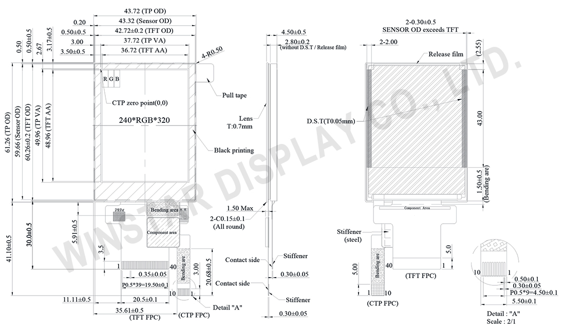
WF24LSYAJDNG0 は、解像度 240x320 ピクセル、輝度 800 ニットを備えた 2.4 インチ縦型 IPS TFT ディスプレイモジュールで、さまざまな照明環境下でも鮮明でクリアな表示を実現します。全方向 80° の広視野角と 800:1 のコントラスト比により、コンパクトな縦型アプリケーションでも鮮やかな画質を提供します。
WF24LSYAJDNG0は投影型静電容量方式タッチパネル(PCAP)が搭載されており、CF1124 タッチコントローラ IC を使用し、I²C インターフェースに対応しています。ディスプレイ部は広く使用されている ILI9341V ドライバ IC により駆動され、80 MCU 8/16/9 ビット並列インターフェースおよび 3 線 9 ビット / 4 線 8 ビット SPI シリアルインターフェースをサポートします。LED バックライトの寿命は 30,000 時間以上で、広い動作温度範囲にも対応しており、携帯機器、医療機器、屋外制御システムなどの縦型タッチ操作用途に最適です。

| 項目 | 仕様 | 単位 |
|---|---|---|
| サイズ (対角線) | 2.4 | インチ |
| ドットマトリックス(解像度) | 240 × RGB × 320(TFT) | dots |
| 外形寸法 | 42.72(W) × 60.26(H) × 4.5(D) | mm |
| 有効エリア | 36.72 × 48.96 | mm |
| ピクセルピッチ | 0.153 × 0.153 | mm |
| LCDタイプ | TFT・ノーマリ・ブラック・透過型 | |
| コントローラー IC | ILI9341V 或いは互換性コントローラー | |
| 視野角度 | 80/80/80/80 | |
| 画面アスペクト比 | ポートレート | |
| バックライトタイプ | LED・ノーマリ・ホワイト | |
| CTP ドライバIC | CF1124或いは互換性IC | |
| CTP インターフェイス | I2C | |
| CTP FW バージョン | 0x01 | |
| CTP 解像度 | 240 * 320 | |
| タッチパネル | 静電容量式タッチパネル | |
| 表面処理 | グレア | |
| 項目 | 記号 | 最小値 | 標準値 | 最大値 | 単位 |
|---|---|---|---|---|---|
| 操作温度 | TOP | -20 | - | +70 | ℃ |
| 保存温度 | TST | -30 | - | +80 | ℃ |
| 項目 | 記号 | 最小値 | 標準値 | 最大値 | 単位 |
|---|---|---|---|---|---|
| アナログ電源電圧 | VCI | 2.5 | — | 3.3 | V |
| ロジック電源電圧 | IOVCC | 2.5 | — | 3.3 | V |
| LCM電源電圧 | ICC | — | 6 | 9 | mA |
| CTP供給 | VDDT | 3.0 | 3.3 | 3.6 | V |
| IDDT | — | 14.0 | 25.0 | mA |
| パラメーター | 記号 | 最小値 | 標準値 | 最大値 | 単位 |
|---|---|---|---|---|---|
| LED電流 | — | — | 40 | — | mA |
| LED電圧 | VBL+ | 10.8 | 11.6 | 12.4 | V |
| LEDの寿命 | — | 30,000 | — | — | Hr |
| NO | 記号 | 功能 | I/O | ||||||||||||||||||||||||||||||||||||||||||||
|---|---|---|---|---|---|---|---|---|---|---|---|---|---|---|---|---|---|---|---|---|---|---|---|---|---|---|---|---|---|---|---|---|---|---|---|---|---|---|---|---|---|---|---|---|---|---|---|
| 1 | GND | Ground | P | ||||||||||||||||||||||||||||||||||||||||||||
| 2-6 | NC | No connection | - | ||||||||||||||||||||||||||||||||||||||||||||
| 7 | VCI | High voltage power supply for analog circuit blocks (2.5 ~ 3.3 V) |
P | ||||||||||||||||||||||||||||||||||||||||||||
| 8 | IOVCC | Low voltage power supply for interface logic circuits (2.5 ~ 3.3 V) |
P | ||||||||||||||||||||||||||||||||||||||||||||
| 9 | TE | Tearing effect output pin to synchronize MPU to frame writing, activated by S/W command. When this pin is not activated, this pin is low. If not used, open this pin. |
O | ||||||||||||||||||||||||||||||||||||||||||||
| 10 | CS | Chip select signal. | I | ||||||||||||||||||||||||||||||||||||||||||||
| 11 | D/CX(SCL) | (D/CX): This pin is used to select “Data or Command” in the parallel interface. When DCX = 1, data is selected. When DCX = 0, command is selected. (SCL): This pin is used as the serial interface clock in 3-wire 9-bit/4-wire 8-bit serial data interface. If not used, this pin should be connected to IOVCC or GND. |
I | ||||||||||||||||||||||||||||||||||||||||||||
| 12 | WR(SPI_D/C) | (WRX) - 8080-Ⅰ/8080-Ⅱ system: Serves as a write signal and writes data at the rising edge. (D/CX) - 4-line system: Serves as the selector of command or parameter. Fix to IOVCC level when not in use. |
I | ||||||||||||||||||||||||||||||||||||||||||||
| 13 | RD | 8080-Ⅰ/8080-Ⅱ system (RDX): Serves as a read signal and MCU read data at the rising edge. Fix to IOVCC level when not in use. |
I | ||||||||||||||||||||||||||||||||||||||||||||
| 14-29 | DB0~DB15 | 18-bit parallel bi-directional data bus for MCU system. Fix to GND level when not in use. |
I/O | ||||||||||||||||||||||||||||||||||||||||||||
| 30 | RESET | This signal will reset the device and must be applied to properly initialize the chip. Signal is active low. |
I | ||||||||||||||||||||||||||||||||||||||||||||
| 31 | IM0 | Select the MCU interface mode
If use RGB Interface must select serial interface. * : Fix this pin at IOVCC or GND. |
I | ||||||||||||||||||||||||||||||||||||||||||||
| 32 | IM1 | ||||||||||||||||||||||||||||||||||||||||||||||
| 33 | IM2 | ||||||||||||||||||||||||||||||||||||||||||||||
| 34 | DB16 | 18-bit parallel bi-directional data bus for MCU system and RGB interface mode Fix to GND level when not in use. |
I/O | ||||||||||||||||||||||||||||||||||||||||||||
| 35 | DB17 | ||||||||||||||||||||||||||||||||||||||||||||||
| 36 | VLED- | Cathode of LED backlight. | P | ||||||||||||||||||||||||||||||||||||||||||||
| 37 | VLED- | Cathode of LED backlight. | P | ||||||||||||||||||||||||||||||||||||||||||||
| 38 | VLED+ | Anode of LED backlight. | P | ||||||||||||||||||||||||||||||||||||||||||||
| 39 | SDA | SDA : Serial in/out signal. The data is applied on the rising edge of the SCL signal. If not used, fix this pin at IOVCC or GND. |
I/O | ||||||||||||||||||||||||||||||||||||||||||||
| 40 | NC | Not used, open this pin | N | ||||||||||||||||||||||||||||||||||||||||||||
| Pin | 記号 | 功能 |
|---|---|---|
| 1 | VSS | Ground for analog circuit |
| 2 | VDDT | Power Supply : +3.3V |
| 3 | SCL | I2C clock input |
| 4 | NC | No connect |
| 5 | SDA | I2C data input and output |
| 6 | NC | No connect |
| 7 | /RST | External Reset, Low is active |
| 8 | NC | No connect |
| 9 | /INT | External interrupt to the host |
| 10 | VSS | Ground for analog circuit |

「すべてのクッキーを許可」をクリックすると、サイトのナビゲーションを向上させ、サイト使用状況を分析し、マーケティングおよびパフォーマンスの取り組みを支援するために、クッキーをデバイスに保存することに同意したことになります。この件に関する詳細情報は、ポリシーをご覧ください。プライバシーポリシー