 - WF24LSYAJDNN0")

우리는 귀하의 프라이버시를 소중히 여깁니다
"모든 쿠키 허용"을 클릭하면 사이트 탐색을 개선하고, 사이트 사용을 분석하며, 마케팅 및 성능 노력에 도움을 주기 위해 쿠키를 귀하의 장치에 저장하는 데 동의한 것으로 간주됩니다. 이 주제에 대한 추가 정보는 당사의 정책에서 확인할 수 있습니다. 개인정보 보호정책

 - WF24LSYAJDNG0")
 - WF24LSYAJDNG0")
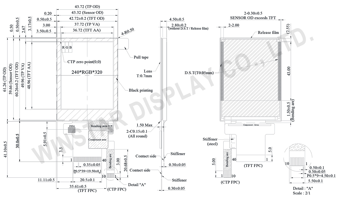
WF24LSYAJDNG0은 240x320 해상도와 800 니트 밝기를 제공하는 2.4인치 세로형 IPS TFT 디스플레이 모듈로, 다양한 조명 환경에서도 선명하고 또렷한 화질을 제공합니다. 전 방향 80°의 광시야각과 800:1의 명암비를 통해, 컴팩트한 세로형 애플리케이션에서도 생생하고 안정적인 이미지를 구현합니다.
이 모델은 정전식 터치 패널(PCAP)을 통합하고, CF1124 터치 컨트롤러 IC를 사용하며, 터치 기능을 위한 I²C 인터페이스를 지원합니다. 디스플레이는 널리 사용되는 ILI9341V 드라이버 IC로 구동되며, 80 MCU 8/16/9비트 병렬 인터페이스와 3선 9비트 / 4선 8비트 SPI 시리얼 인터페이스를 지원합니다. LED 백라이트 수명은 30,000시간 이상이며, 넓은 동작 온도 범위 덕분에 휴대용 장치, 의료 기기, 실외 제어 시스템 등 직관적인 터치 조작이 필요한 세로형 응용에 적합합니다.

| 항목 | 치수 | 단위 |
|---|---|---|
| 크기 (대각선) | 2.4 | 인치 |
| 도트 매트릭스 (해상도) | 240 × RGB × 320(TFT) | dots |
| 모듈 치수 | 42.72(W) × 60.26(H) × 4.5(D) | mm |
| 활성 영역 | 36.72 × 48.96 | mm |
| 도트 피치 | 0.153 × 0.153 | mm |
| LCD 유형 | TFT, 검은색, 투과성 | |
| 제어 IC | ILI9341V 또는 이와 동등한 | |
| 시야각 | 80/80/80/80 | |
| 종횡비 | 세로 모드 | |
| 역광 타입 | LED,백색 | |
| CTP 드라이버 IC | CF1124 또는 이와 동등한 | |
| CTP 인터페이스 | I2C | |
| CTP FW 버전 | 0x01 | |
| CTP 해상도 | 240 * 320 | |
| 터치 패널 | 용량식 터치패널이 있는 (CTP) | |
| 표면 | 눈부심 | |
| 항목 | 기호 | 최소값 | 대표값 | 최대값 | 단위 |
|---|---|---|---|---|---|
| 작동 온도 | TOP | -20 | - | +70 | ℃ |
| 보관 온도 | TST | -30 | - | +80 | ℃ |
| 항목 | 기호 | 최소값 | 대표값 | 최대값 | 단위 |
|---|---|---|---|---|---|
| Supply Voltage For Analog | VCI | 2.5 | — | 3.3 | V |
| Supply Voltage For Logic | IOVCC | 2.5 | — | 3.3 | V |
| Supply Current For LCM | ICC | — | 6 | 9 | mA |
| Supply CTP | VDDT | 3.0 | 3.3 | 3.6 | V |
| IDDT | — | 14.0 | 25.0 | mA |
| 매개변수 | 기호 | 최소값 | 대표값 | 최대값 | 단위 |
|---|---|---|---|---|---|
| LED 전류 | — | — | 40 | — | mA |
| LED 전압 | VBL+ | 10.8 | 11.6 | 12.4 | V |
| LED 수명 | — | 30,000 | — | — | Hr |
| NO | 기호 | 기능 | I/O | ||||||||||||||||||||||||||||||||||||||||||||
|---|---|---|---|---|---|---|---|---|---|---|---|---|---|---|---|---|---|---|---|---|---|---|---|---|---|---|---|---|---|---|---|---|---|---|---|---|---|---|---|---|---|---|---|---|---|---|---|
| 1 | GND | Ground | P | ||||||||||||||||||||||||||||||||||||||||||||
| 2-6 | NC | No connection | - | ||||||||||||||||||||||||||||||||||||||||||||
| 7 | VCI | High voltage power supply for analog circuit blocks (2.5 ~ 3.3 V) |
P | ||||||||||||||||||||||||||||||||||||||||||||
| 8 | IOVCC | Low voltage power supply for interface logic circuits (2.5 ~ 3.3 V) |
P | ||||||||||||||||||||||||||||||||||||||||||||
| 9 | TE | Tearing effect output pin to synchronize MPU to frame writing, activated by S/W command. When this pin is not activated, this pin is low. If not used, open this pin. |
O | ||||||||||||||||||||||||||||||||||||||||||||
| 10 | CS | Chip select signal. | I | ||||||||||||||||||||||||||||||||||||||||||||
| 11 | D/CX(SCL) | (D/CX): This pin is used to select “Data or Command” in the parallel interface. When DCX = 1, data is selected. When DCX = 0, command is selected. (SCL): This pin is used as the serial interface clock in 3-wire 9-bit/4-wire 8-bit serial data interface. If not used, this pin should be connected to IOVCC or GND. |
I | ||||||||||||||||||||||||||||||||||||||||||||
| 12 | WR(SPI_D/C) | (WRX) - 8080-Ⅰ/8080-Ⅱ system: Serves as a write signal and writes data at the rising edge. (D/CX) - 4-line system: Serves as the selector of command or parameter. Fix to IOVCC level when not in use. |
I | ||||||||||||||||||||||||||||||||||||||||||||
| 13 | RD | 8080-Ⅰ/8080-Ⅱ system (RDX): Serves as a read signal and MCU read data at the rising edge. Fix to IOVCC level when not in use. |
I | ||||||||||||||||||||||||||||||||||||||||||||
| 14-29 | DB0~DB15 | 18-bit parallel bi-directional data bus for MCU system. Fix to GND level when not in use. |
I/O | ||||||||||||||||||||||||||||||||||||||||||||
| 30 | RESET | This signal will reset the device and must be applied to properly initialize the chip. Signal is active low. |
I | ||||||||||||||||||||||||||||||||||||||||||||
| 31 | IM0 | Select the MCU interface mode
If use RGB Interface must select serial interface. * : Fix this pin at IOVCC or GND. |
I | ||||||||||||||||||||||||||||||||||||||||||||
| 32 | IM1 | ||||||||||||||||||||||||||||||||||||||||||||||
| 33 | IM2 | ||||||||||||||||||||||||||||||||||||||||||||||
| 34 | DB16 | 18-bit parallel bi-directional data bus for MCU system and RGB interface mode Fix to GND level when not in use. |
I/O | ||||||||||||||||||||||||||||||||||||||||||||
| 35 | DB17 | ||||||||||||||||||||||||||||||||||||||||||||||
| 36 | VLED- | Cathode of LED backlight. | P | ||||||||||||||||||||||||||||||||||||||||||||
| 37 | VLED- | Cathode of LED backlight. | P | ||||||||||||||||||||||||||||||||||||||||||||
| 38 | VLED+ | Anode of LED backlight. | P | ||||||||||||||||||||||||||||||||||||||||||||
| 39 | SDA | SDA : Serial in/out signal. The data is applied on the rising edge of the SCL signal. If not used, fix this pin at IOVCC or GND. |
I/O | ||||||||||||||||||||||||||||||||||||||||||||
| 40 | NC | Not used, open this pin | N | ||||||||||||||||||||||||||||||||||||||||||||
| Pin | 기호 | 기능 |
|---|---|---|
| 1 | VSS | Ground for analog circuit |
| 2 | VDDT | Power Supply : +3.3V |
| 3 | SCL | I2C clock input |
| 4 | NC | No connect |
| 5 | SDA | I2C data input and output |
| 6 | NC | No connect |
| 7 | /RST | External Reset, Low is active |
| 8 | NC | No connect |
| 9 | /INT | External interrupt to the host |
| 10 | VSS | Ground for analog circuit |

"모든 쿠키 허용"을 클릭하면 사이트 탐색을 개선하고, 사이트 사용을 분석하며, 마케팅 및 성능 노력에 도움을 주기 위해 쿠키를 귀하의 장치에 저장하는 데 동의한 것으로 간주됩니다. 이 주제에 대한 추가 정보는 당사의 정책에서 확인할 수 있습니다. 개인정보 보호정책