
 - WEP012864AJ(RS232)")

私たちはあなたのプライバシーを大切にします
「すべてのクッキーを許可」をクリックすると、サイトのナビゲーションを向上させ、サイト使用状況を分析し、マーケティングおよびパフォーマンスの取り組みを支援するために、クッキーをデバイスに保存することに同意したことになります。この件に関する詳細情報は、ポリシーをご覧ください。プライバシーポリシー

 - WEP012864AJ")
 - WEP012864AJ")
 - WEP012864AJ")
 - WEP012864AJ")
 - WEP012864AJ")
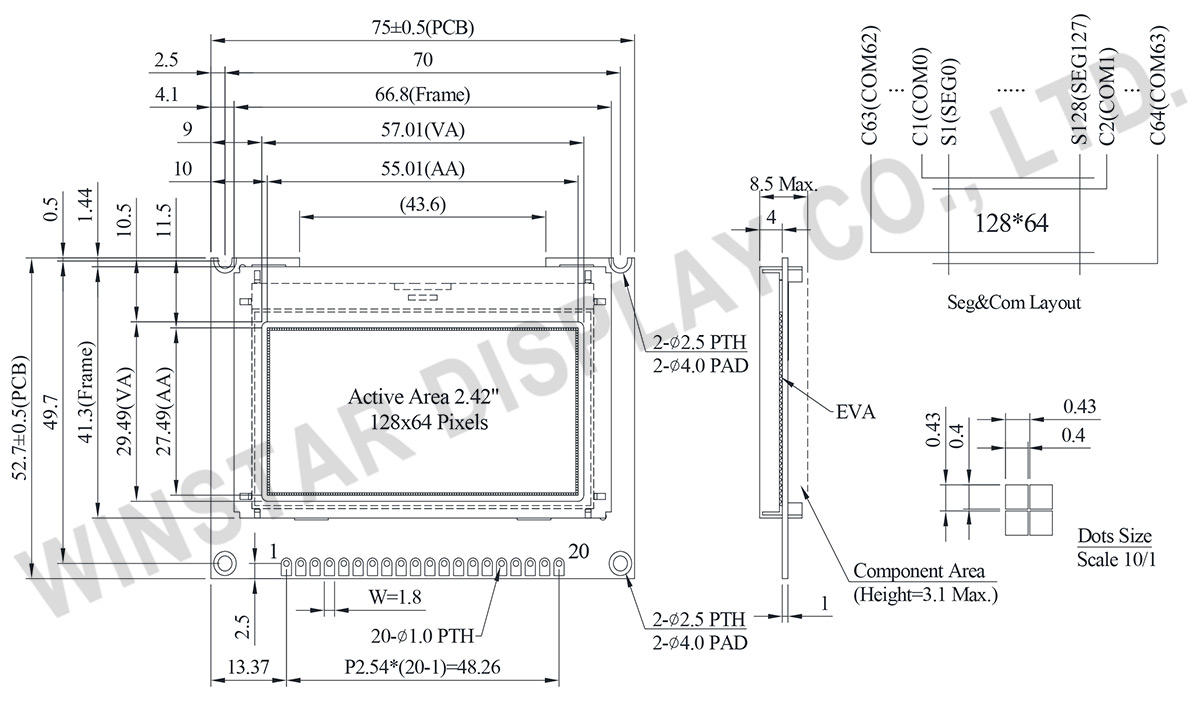
WEP012864AJは、128x64ドットマトリックス解像度を持つ2.42インチ単色グラフィック有機EL(OLED)モジュールです。このバージョンは8080 8-bit パラレルインタフェースに対応しており、高速データ転送による低遅延な画面更新を実現します。COG + フレーム + PCBの一体型構造により、機械的耐久性に優れ、装置への組み込みも容易です。
Data source ref:WEP012864AJLPP3N00000
| 項目 | 仕様 | 単位 |
|---|---|---|
| ドットマトリックス(解像度) | 128 x 64 | - |
| モジュールサイズ | 75.0 × 52.7 × 8.5(Max). | mm |
| 有効エリア | 55.01 × 27.49 | mm |
| ドットサイズ | 0.40 × 0.40 | mm |
| ドットピッチ | 0.43 × 0.43 | mm |
| 表示モード | パッシブマトリクス | |
| 表示カラー | モノクロ | |
| 駆動方法 | 1/64 Duty | |
| IC | CH1116 | |
| インターフェース | 8080 | |
| サイズ | 2.42 インチ | |
| パラメーター | 記号 | 最小値 | 最大値 | 単位 |
|---|---|---|---|---|
| ロジック電源電圧 | VDD | -0.3 | 3.6 | V |
| 操作温度 | TOP | -40 | +80 | °C |
| 保存温度 | TSTG | -40 | +85 | °C |
| 項目 | 記号 | 条件 | 最小値 | 典型値 | 最大値 | 単位 |
|---|---|---|---|---|---|---|
| ロジック電源電圧 | VDD | - | 2.8 | 3.0 | 3.3 | V |
| 高レベル入力 | VIH | - | 0.8×VDD | - | VDD | V |
| 低レベル入力 | VIL | - | VSS | - | 0.2×VDD | V |
| 高レベル出力 | VOH | - | 0.8×VDD | - | VDD | V |
| 低レベル出力 | VOL | - | VSS | - | 0.2×VDD | V |
| ディスプレイ 50% ピクセルオン | IDD | VDD =3.0V | - | 60 | 120 | mA |
| No. | 符号 | 説明 |
|---|---|---|
| 1 | VDD | Power supply input |
| 2 | VSS | Ground. |
| 3 | NC | No connection |
| 4~11 | D0~D7 | This is an 8-bit bi-directional data bus that connects to an 8-bit or 16-bit standard MPU data bus. |
| 12 | CS# | This pad is the chip select input. When="L", then the chip select becomes active, and data/command I/O is enabled. |
| 13 | NC | No Connection |
| 14 | RES# | This is a reset signal input pad. When is set to "L", the settings are initialized. The reset operation is performed by the signal level. |
| 15 | W/R# | This is a MPU interface input pad. When connected to an 8080 MPU, this is active LOW. This pad connects to the 8080 MPU signal. The signals on the data bus are latched at the rising edge of the signal. |
| 16 | A0 | This is the Data/Command control pad that determines whether the data bits are data or a command. A0="H": the inputs at D0 to D7 are treated as display data. A0="L": the inputs at D0 to D7 are transferred to the command registers. |
| 17 | R/D# | This is a MPU interface input pad. When connected to an 8080 series MPU, it is active LOW. This pad is connected to the signal of the 8080 series MPU, and the data bus is in an output status when this signal is "L". |
| 18 | NC | No Connection |
| 19 | DISP | Display off when it's pulled low; Display on when it's pulled high. |
| 20 | NC | No connection |

「すべてのクッキーを許可」をクリックすると、サイトのナビゲーションを向上させ、サイト使用状況を分析し、マーケティングおよびパフォーマンスの取り組みを支援するために、クッキーをデバイスに保存することに同意したことになります。この件に関する詳細情報は、ポリシーをご覧ください。プライバシーポリシー