
私たちはあなたのプライバシーを大切にします
「すべてのクッキーを許可」をクリックすると、サイトのナビゲーションを向上させ、サイト使用状況を分析し、マーケティングおよびパフォーマンスの取り組みを支援するために、クッキーをデバイスに保存することに同意したことになります。この件に関する詳細情報は、ポリシーをご覧ください。プライバシーポリシー


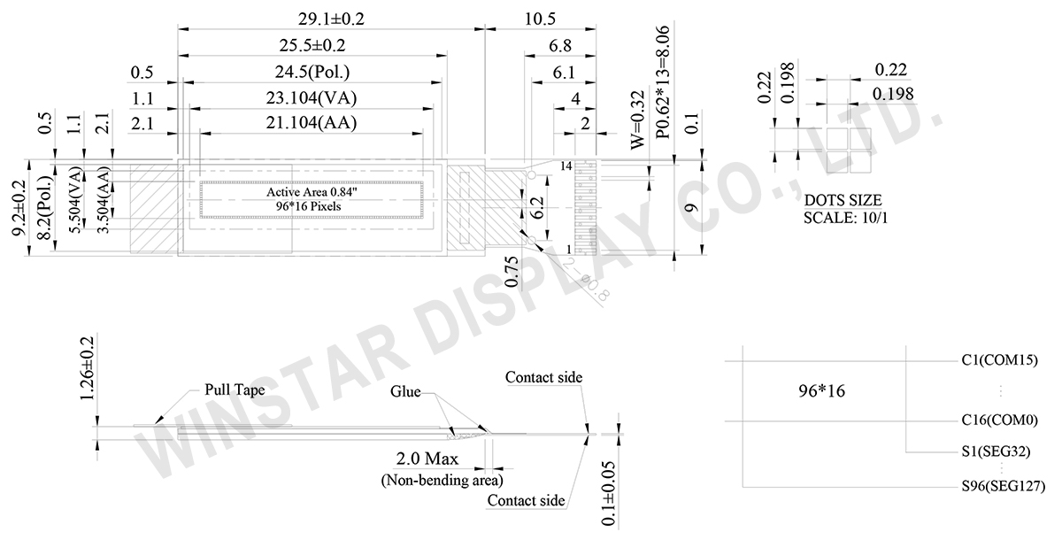
WEO009616A は、0.84インチOLEDディスプレイモジュールで、96x16の解像度を提供し、コンパクトで高性能なディスプレイが求められるアプリケーションに最適です。COG(Chip-on-Glass)デザインにより、このOLEDディスプレイは超薄型で自発光型(バックライト不要)、エネルギー効率が良く、優れた明瞭さと低消費電力を実現しています。また、SSD1306コントローラを内蔵し、I2Cインターフェースをサポートしており、さまざまな組み込みシステムやデバイスへの統合が容易です。
この96x16 OLEDディスプレイは、コンパクトで効率的なディスプレイが求められるさまざまなアプリケーションに最適です:
Data source ref: WEO009616AWPP3N00000
| 項目 | 仕様 | 単位 |
|---|---|---|
| ドットマトリックス | 96 x 16 Dots | - |
| モジュールサイズ | 29.1× 9.2 × 1.26 | mm |
| アクティブエリア | 21.104 × 3.504 | mm |
| ピクセルサイズ | 0.198 × 0.198 | mm |
| ピクセルピッチ | 0.220 × 0.220 | mm |
| 表示モード | パッシブマトリクス(Passive Matrix) | |
| 表示カラー | モノクロ | |
| 駆動方法 | 1/16 Duty | |
| IC | SSD1306 | |
| インターフェイス | I2C | |
| 表示サイズ(対角線) | 0.84 インチ | |
| パラメーター | 記号 | 最小値 | 最大値 | 単位 |
|---|---|---|---|---|
| ロジック電源電圧 | VDD | 0 | 4.0 | V |
| 表示用電源電圧 | VCC | 0 | 16.0 | V |
| 操作温度 | TOP | -40 | +80 | °C |
| 保存温度 | TSTG | -40 | +85 | °C |
| 項目 | 記号 | 条件 | 最小値 | 典型値 | 最大値 | 単位 |
|---|---|---|---|---|---|---|
| ロジック電源電圧 | VDD | - | 1.65 | 3.0 | 3.3 | V |
| ディスプレイの供給電圧(外部供給) | VCC | - | 7.0 | 7.5 | 7.8 | V |
| チャージポンプレギュレータ供給電圧 | VBAT | - | 3.3 | - | 4.2 | V |
| チャージポンプ出力電圧(内部DC/DC生成) | Charge Pump VCC |
- | 7.0 | 7.5 | 7.8 | V |
| 高レベル入力電圧 | VIH | - | 0.8×VDD | - | VDD | V |
| 低レベル入力電圧 | VIL | - | 0 | - | 0.2×VDD | V |
| 高レベル出力電圧 | VOH | - | 0.9×VDD | - | VDD | V |
| 低レベル出力電圧 | VOL | - | 0 | - | 0.1×VDD | V |
| 50% チェックボード動作電流(VCC 外部供給) | ICC | - | - | 7 | 15 | mA |
| 50% チェックボード動作電流(VCC 内部DC/DC生成) | IBAT | - | 10 | 15 | 25 | mA |
| No. | 記号 | 説明 |
|---|---|---|
| 1 | C2N | Positive Terminal of the Flying Inverting CapacitorNegative Terminal of the Flying Boost Capacitor The charge-pump capacitors are required between the terminals. They must be floated when the converter is not used. |
| 2 | C2P | |
| 3 | C1P | |
| 4 | C1N | |
| 5 | VBAT | Power Supply for DC/DC Converter Circuit This is the power supply pin for the internal buffer of the DC/DC voltage converter. It must be connected to external source when the converter is used. It should be connected to VDD when the converter is not used. |
| 6 | NC | No connection |
| 7 | VSS | Ground of Logic Circuit This is a ground pin. It acts as a reference for the logic pins. It must be connected to external ground. |
| 8 | VDD | Power Supply for Logic This is a voltage supply pin. It must be connected to external source. |
| 9 | RES# | Power Reset for Controller and Driver This pin is reset signal input. When the pin is low, initialization of the chip is executed. |
| 10 | SCL | I2C mode is selected, D2, D1 should be tied together and serve as SDAout, SDAin inapplication and D0 is the serial clock input, SCL. |
| 11 | SDA | |
| 12 | IREF | Current Reference for Brightness Adjustment This pin is segment current reference pin. A resistor should be connected between this pin and VSS. Set the current lower than 30uA. |
| 13 | VCOMH | Voltage Output High Level for COM Signal This pin is the input pin for the voltage output high level for COM signals. A capacitor should be connected between this pin and VSS. |
| 14 | VCC | Power Supply for OEL Panel This is the most positive voltage supply pin of the chip. A stabilization capacitor should be connected between this pin and VSS when the converter is used. It must be connected to external source when the converter is not used. |

「すべてのクッキーを許可」をクリックすると、サイトのナビゲーションを向上させ、サイト使用状況を分析し、マーケティングおよびパフォーマンスの取り組みを支援するために、クッキーをデバイスに保存することに同意したことになります。この件に関する詳細情報は、ポリシーをご覧ください。プライバシーポリシー