我们重视您的隐私
通过点击「允许所有 Cookie」,代表您同意在您的设备上存储 Cookie 以增强网站浏览体验、分析网站使用情况并协助我们的营销和网站效能优化工作。您可以在我们的隐私权政策中找到有关于此的更多信息。


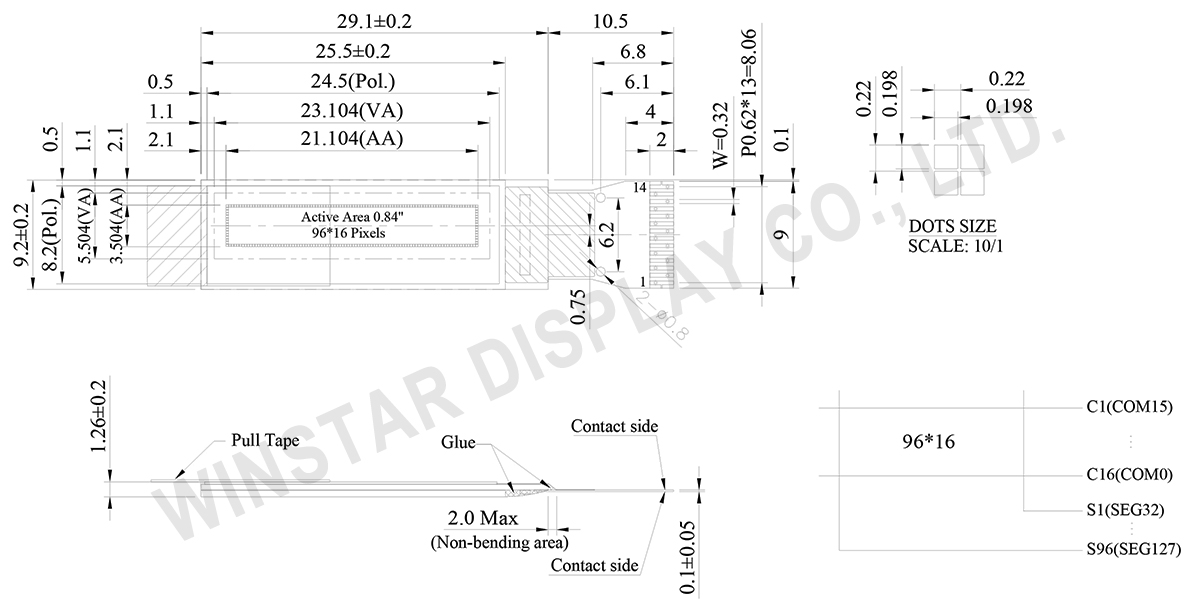
WEO009616A 是一款 0.84英寸 OLED 显示模块,具有 96x16 分辨率,非常适合需要紧凑且高性能显示的应用。采用 COG(Chip-on-Glass)设计,该 OLED 显示器超薄,具备自发光特性(无需背光),节能高效,提供卓越的清晰度和低功耗。此模块内置 SSD1306 控制器,并支持 I2C 接口,便于与各种嵌入式系统和设备进行集成。
这款 96x16 OLED 显示屏 非常适合需要紧凑、高效显示的多种应用:
Data source ref: WEO009616AWPP3N00000
| 项目 | 尺寸 | 单位 |
|---|---|---|
| 点阵 | 96 x 16 Dots | - |
| 模块尺寸 | 29.1× 9.2 × 1.26 | mm |
| 有效区域 | 21.104 × 3.504 | mm |
| 像素大小 | 0.198 × 0.198 | mm |
| 像素间距 | 0.220 × 0.220 | mm |
| 显示模式 | 被动矩阵(Passive Matrix) | |
| 显示颜色 | 单色 | |
| 驱动方式 | 1/16 Duty | |
| IC | SSD1306 | |
| 接口 | I2C | |
| 对角线尺寸 | 0.84 寸 | |
| 参数 | 符号 | 最小值 | 最大值 | 单位 |
|---|---|---|---|---|
| 逻辑电源电压 | VDD | 0 | 4.0 | V |
| 显示电源电压 | VCC | 0 | 16.0 | V |
| 工作温度 | TOP | -40 | +80 | °C |
| 储存温度 | TSTG | -40 | +85 | °C |
| 项目 | 符号 | 条件 | 最小值 | 典型值 | 最大值 | 单位 |
|---|---|---|---|---|---|---|
| 逻辑电源电压 | VDD | - | 1.65 | 3.0 | 3.3 | V |
| 显示器供电电压(外部供应) | VCC | - | 7.0 | 7.5 | 7.8 | V |
| 电荷帮浦稳压器电源电压 | VBAT | - | 3.3 | - | 4.2 | V |
| 显示器的电荷帮浦输出电压(由内部DC/DC生成) | Charge Pump VCC |
- | 7.0 | 7.5 | 7.8 | V |
| 输入高电压 | VIH | - | 0.8×VDD | - | VDD | V |
| 输入低电压 | VIL | - | 0 | - | 0.2×VDD | V |
| 输出高电压 | VOH | - | 0.9×VDD | - | VDD | V |
| 输出低电压 | VOL | - | 0 | - | 0.1×VDD | V |
| 50% 设备运行电流(VCC 外部供应) | ICC | - | - | 7 | 15 | mA |
| 50% 设备运行电流(VCC 由内部 DC/DC 生成) | IBAT | - | 10 | 15 | 25 | mA |
| No. | 符号 | 功能说明 |
|---|---|---|
| 1 | C2N | Positive Terminal of the Flying Inverting CapacitorNegative Terminal of the Flying Boost Capacitor The charge-pump capacitors are required between the terminals. They must be floated when the converter is not used. |
| 2 | C2P | |
| 3 | C1P | |
| 4 | C1N | |
| 5 | VBAT | Power Supply for DC/DC Converter Circuit This is the power supply pin for the internal buffer of the DC/DC voltage converter. It must be connected to external source when the converter is used. It should be connected to VDD when the converter is not used. |
| 6 | NC | No connection |
| 7 | VSS | Ground of Logic Circuit This is a ground pin. It acts as a reference for the logic pins. It must be connected to external ground. |
| 8 | VDD | Power Supply for Logic This is a voltage supply pin. It must be connected to external source. |
| 9 | RES# | Power Reset for Controller and Driver This pin is reset signal input. When the pin is low, initialization of the chip is executed. |
| 10 | SCL | I2C mode is selected, D2, D1 should be tied together and serve as SDAout, SDAin inapplication and D0 is the serial clock input, SCL. |
| 11 | SDA | |
| 12 | IREF | Current Reference for Brightness Adjustment This pin is segment current reference pin. A resistor should be connected between this pin and VSS. Set the current lower than 30uA. |
| 13 | VCOMH | Voltage Output High Level for COM Signal This pin is the input pin for the voltage output high level for COM signals. A capacitor should be connected between this pin and VSS. |
| 14 | VCC | Power Supply for OEL Panel This is the most positive voltage supply pin of the chip. A stabilization capacitor should be connected between this pin and VSS when the converter is used. It must be connected to external source when the converter is not used. |

通过点击「允许所有 Cookie」,代表您同意在您的设备上存储 Cookie 以增强网站浏览体验、分析网站使用情况并协助我们的营销和网站效能优化工作。您可以在我们的隐私权政策中找到有关于此的更多信息。