우리는 귀하의 프라이버시를 소중히 여깁니다
"모든 쿠키 허용"을 클릭하면 사이트 탐색을 개선하고, 사이트 사용을 분석하며, 마케팅 및 성능 노력에 도움을 주기 위해 쿠키를 귀하의 장치에 저장하는 데 동의한 것으로 간주됩니다. 이 주제에 대한 추가 정보는 당사의 정책에서 확인할 수 있습니다. 개인정보 보호정책


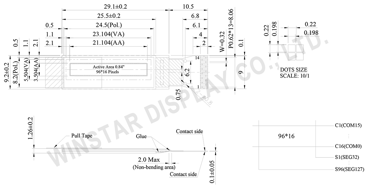
WEO009616A는 0.84인치 OLED 디스플레이 모듈로, 96x16 해상도를 제공하며, 컴팩트하고 고성능 디스플레이가 요구되는 애플리케이션에 적합합니다. COG(Chip-on-Glass) 디자인을 채택하여 이 OLED 디스플레이는 초박형이며, 백라이트가 필요 없는 자발광형으로 에너지 효율이 뛰어나며, 뛰어난 선명도와 낮은 전력 소비를 제공합니다. 이 모듈은 SSD1306 컨트롤러를 내장하고 있으며 I2C 인터페이스를 지원하여 다양한 임베디드 시스템 및 장치에 쉽게 통합할 수 있습니다.
이 96x16 OLED 디스플레이는 컴팩트하고 효율적인 디스플레이가 필요한 다양한 애플리케이션에 적합합니다:
Data source ref: WEO009616AWPP3N00000
| 항목 | 치수 | 단위 |
|---|---|---|
| 도트 매트릭스 | 96 x 16 Dots | - |
| 모듈 치수 | 29.1× 9.2 × 1.26 | mm |
| 활성 영역 | 21.104 × 3.504 | mm |
| 픽셀 크기 | 0.198 × 0.198 | mm |
| 픽셀 피치 | 0.220 × 0.220 | mm |
| 디스플레이 모드 | 패시브 매트릭스 (Passive Matrix) | |
| 디스플레이 색상 | 단색 | |
| 구동 듀티 | 1/16 Duty | |
| IC | SSD1306 | |
| 인터페이스 | I2C | |
| 크기 (대각선) | 0.84 인치 | |
| 매개변수 | 기호 | 최소값 | 최대값 | 단위 |
|---|---|---|---|---|
| 논리 회로 공급 전압 | VDD | 0 | 4.0 | V |
| 디스플레이 전원 공급 전압 | VCC | 0 | 16.0 | V |
| 작동 온도 | TOP | -40 | +80 | °C |
| 보관 온도 | TSTG | -40 | +85 | °C |
| 항목 | 기호 | 조건 | 최소값 | 대표값 | 최대값 | 단위 |
|---|---|---|---|---|---|---|
| 논리용 전원 공급 전압 | VDD | - | 1.65 | 3.0 | 3.3 | V |
| 디스플레이 전원 공급 전압 (외부 공급) | VCC | - | 7.0 | 7.5 | 7.8 | V |
| 차지 펌프 레귤레이터 전원 공급 전압 | VBAT | - | 3.3 | - | 4.2 | V |
| 디스플레이 차지 펌프 출력 전압 (내부 DC/DC 생성) | Charge Pump VCC |
- | 7.0 | 7.5 | 7.8 | V |
| 입력 고전압 | VIH | - | 0.8×VDD | - | VDD | V |
| 입력 저전압 | VIL | - | 0 | - | 0.2×VDD | V |
| 출력 고전압 | VOH | - | 0.9×VDD | - | VDD | V |
| 출력 저전압 | VOL | - | 0 | - | 0.1×VDD | V |
| 50% 보드 동작 전류 (VCC 외부 공급) | ICC | - | - | 7 | 15 | mA |
| 50% 보드 동작 전류 (VCC 내부 DC/DC 생성) | IBAT | - | 10 | 15 | 25 | mA |
| No. | 기호 | 기능 |
|---|---|---|
| 1 | C2N | Positive Terminal of the Flying Inverting CapacitorNegative Terminal of the Flying Boost Capacitor The charge-pump capacitors are required between the terminals. They must be floated when the converter is not used. |
| 2 | C2P | |
| 3 | C1P | |
| 4 | C1N | |
| 5 | VBAT | Power Supply for DC/DC Converter Circuit This is the power supply pin for the internal buffer of the DC/DC voltage converter. It must be connected to external source when the converter is used. It should be connected to VDD when the converter is not used. |
| 6 | NC | No connection |
| 7 | VSS | Ground of Logic Circuit This is a ground pin. It acts as a reference for the logic pins. It must be connected to external ground. |
| 8 | VDD | Power Supply for Logic This is a voltage supply pin. It must be connected to external source. |
| 9 | RES# | Power Reset for Controller and Driver This pin is reset signal input. When the pin is low, initialization of the chip is executed. |
| 10 | SCL | I2C mode is selected, D2, D1 should be tied together and serve as SDAout, SDAin inapplication and D0 is the serial clock input, SCL. |
| 11 | SDA | |
| 12 | IREF | Current Reference for Brightness Adjustment This pin is segment current reference pin. A resistor should be connected between this pin and VSS. Set the current lower than 30uA. |
| 13 | VCOMH | Voltage Output High Level for COM Signal This pin is the input pin for the voltage output high level for COM signals. A capacitor should be connected between this pin and VSS. |
| 14 | VCC | Power Supply for OEL Panel This is the most positive voltage supply pin of the chip. A stabilization capacitor should be connected between this pin and VSS when the converter is used. It must be connected to external source when the converter is not used. |

"모든 쿠키 허용"을 클릭하면 사이트 탐색을 개선하고, 사이트 사용을 분석하며, 마케팅 및 성능 노력에 도움을 주기 위해 쿠키를 귀하의 장치에 저장하는 데 동의한 것으로 간주됩니다. 이 주제에 대한 추가 정보는 당사의 정책에서 확인할 수 있습니다. 개인정보 보호정책