

私たちはあなたのプライバシーを大切にします
「すべてのクッキーを許可」をクリックすると、サイトのナビゲーションを向上させ、サイト使用状況を分析し、マーケティングおよびパフォーマンスの取り組みを支援するために、クッキーをデバイスに保存することに同意したことになります。この件に関する詳細情報は、ポリシーをご覧ください。プライバシーポリシー


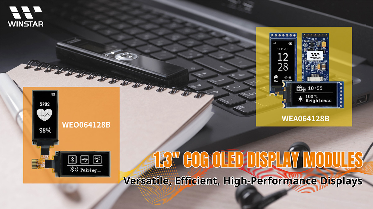
WEO064128Bシリーズの1.3インチOLEDディスプレイモジュールは、卓越した性能と柔軟な統合能力を提供し、ゲーミング周辺機器、スマートホームデバイス、産業用制御システムなど、多様なニーズに対応します。その高いコントラスト比、信頼性、低消費電力設計により、高効率な製品を設計するエンジニアにとって理想的な選択肢です。
WEO064128Bシリーズの1.3インチOLEDディスプレイモジュールは、その高品質と安定した性能により、多領域の設計課題を容易に克服し、製品開発を加速します。ゲーミング、スマートホーム、産業用途のいずれに焦点を当てていても、このモジュールはニーズに応えます。
詳細情報を知りたい方は、ぜひお問い合わせください。次世代の製品設計に革新をもたらしましょう!
Data source ref: WEO064128BWAP3N00000
| 項目 | 仕様 | 単位 |
|---|---|---|
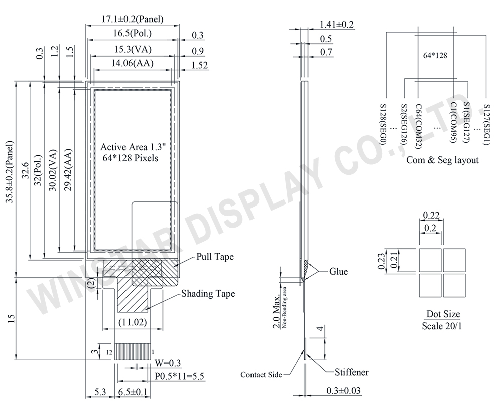
| ドットマトリックス(解像度) | 64 x 128 | Dots |
| 外形寸法 | 17.1 × 35.80 × 1.41 | mm |
| 有効表示エリア | 14.06 × 29.42 | mm |
| ピクセルサイズ | 0.20 × 0.21 | mm |
| ピクセルピッチ | 0.22 × 0.23 | mm |
| 表示モード | パッシブマトリクス | |
| 発光色 | モノクロ | |
| 駆動方法 | 1/64 Duty | |
| IC | SH1107 | |
| インターフェイス | 4-wire SPI , I2C | |
| サイズ | 1.3 インチ | |
| パラメーター | 記号 | 最小値 | 最大値 | 単位 |
|---|---|---|---|---|
| ロジック電源電圧 | VDD | -0.3 | 3.6 | V |
| Display電源電圧 | VPP | 7.0 | 17.0 | V |
| 操作温度 | TOP | -40 | +80 | °C |
| 保存温度 | TSTG | -40 | +85 | °C |
| 項目 | 記号 | 条件 | 最小値 | 典型値 | 最大値 | 単位 |
|---|---|---|---|---|---|---|
| ロジック電源電圧 | VDD | - | 1.65 | 3.0 | 3.5 | V |
| Display電源電圧 | VPP | - | 7.0 | 13.0 | 13.5 | V |
| 入力電圧(High) | VIH | - | 0.8×VDD | - | VDD | V |
| 入力電圧(Low) | VIL | - | VSS | - | 0.2×VDD | V |
| 出力電圧(High) | VOH | - | 0.8×VDD | - | VDD | V |
| 出力電圧(Low) | VOL | - | VSS | - | 0.2×VDD | V |
| Display 50% Pixel on | IPP | VPP=13V | - | 10 | 15 | mA |
| No. | 記号 | 説明 |
|---|---|---|
| 1 | VSS | Ground. |
| 2 | D1 | When the serial interface is selected, then D0 serves as the serial clock input pad (SCL) and D1 serves as the serial data input pad (SI). When the I2C interface is selected, then D0 serves as the serial clock input pad (SCL) and D1 serves as the serial data input pad (SDA). |
| 3 | D0 | |
| 4 | A0 | This is the Data/Command control pad that determines whether the data bits are data or a command. A0 = “H”: Data. A0 = “L”: Command In I2C interface, this pad serves as SA0 to distinguish the different address of OLED driver. |
| 5 | ___ RES |
This is a reset signal input pad. When RES is set to “L”, the settings are initialized. The reset operation is performed by the RES signal level. |
| 6 | __ CS |
This pad is the chip select input. When CS = “L”, then the chip select becomes active, and data/command I/O is enabled. |
| 7 | IREF | This is a segment current reference pad. A resistor should be connected between this pad and VSS. Set the current at 15.625uA. |
| 8 | IM1 | These are the MPU interface mode select pads. IM1 connect to VDD is I2C interface. IM1 connect to VSS is 4-wire SPI interface. |
| 9 | VDD | Power supply for logic and input. |
| 10 | VCOMH | This is a pad for the voltage output high level for common signals. A capacitor should be connected between this pad and VSS. |
| 11 | VPP | This is the most positive voltage supply pad of the chip. It should be supplied externally. |
| 12 | VSS | Ground. |

「すべてのクッキーを許可」をクリックすると、サイトのナビゲーションを向上させ、サイト使用状況を分析し、マーケティングおよびパフォーマンスの取り組みを支援するために、クッキーをデバイスに保存することに同意したことになります。この件に関する詳細情報は、ポリシーをご覧ください。プライバシーポリシー