
我们重视您的隐私
通过点击「允许所有 Cookie」,代表您同意在您的设备上存储 Cookie 以增强网站浏览体验、分析网站使用情况并协助我们的营销和网站效能优化工作。您可以在我们的隐私权政策中找到有关于此的更多信息。


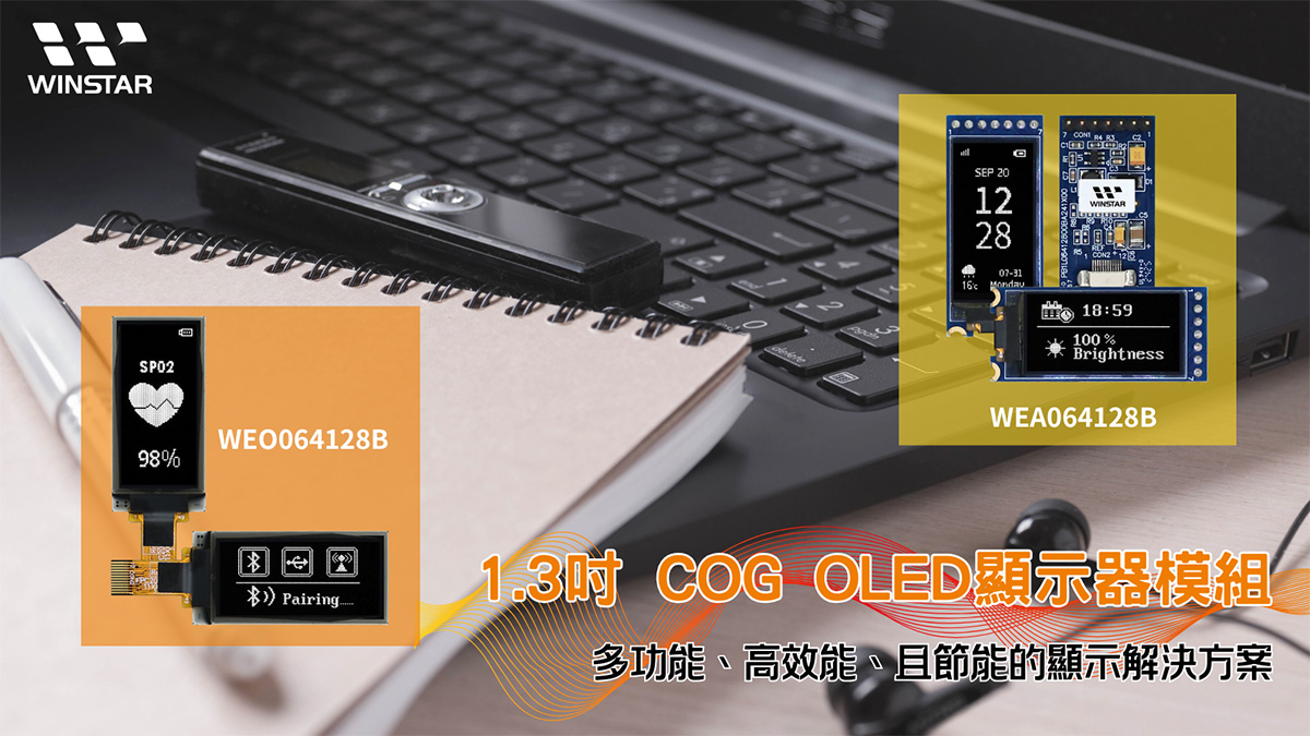
WEO064128B系列1.3吋OLED显示器模块,以卓越的性能和灵活的整合能力,满足从电竞设备到智能家居和工业控制等多元应用需求。其高对比度度、稳定性与低功耗设计,成为研发人员设计高效产品的不二选择。
WEO064128B系列1.3吋OLED显示器模块 的高质量与稳定性能,助您轻松应对多领域设计挑战,快速实现产品开发目标。无论是专注于电竞市场,还是智能家居与工业应用,此模块都能完美契合您的需求。
立即联系我们,探索更多可能,为您的下一代产品设计提供完美支持!
Data source ref: WEO064128BWAP3N00000
| 项目 | 规格 | 单位 |
|---|---|---|
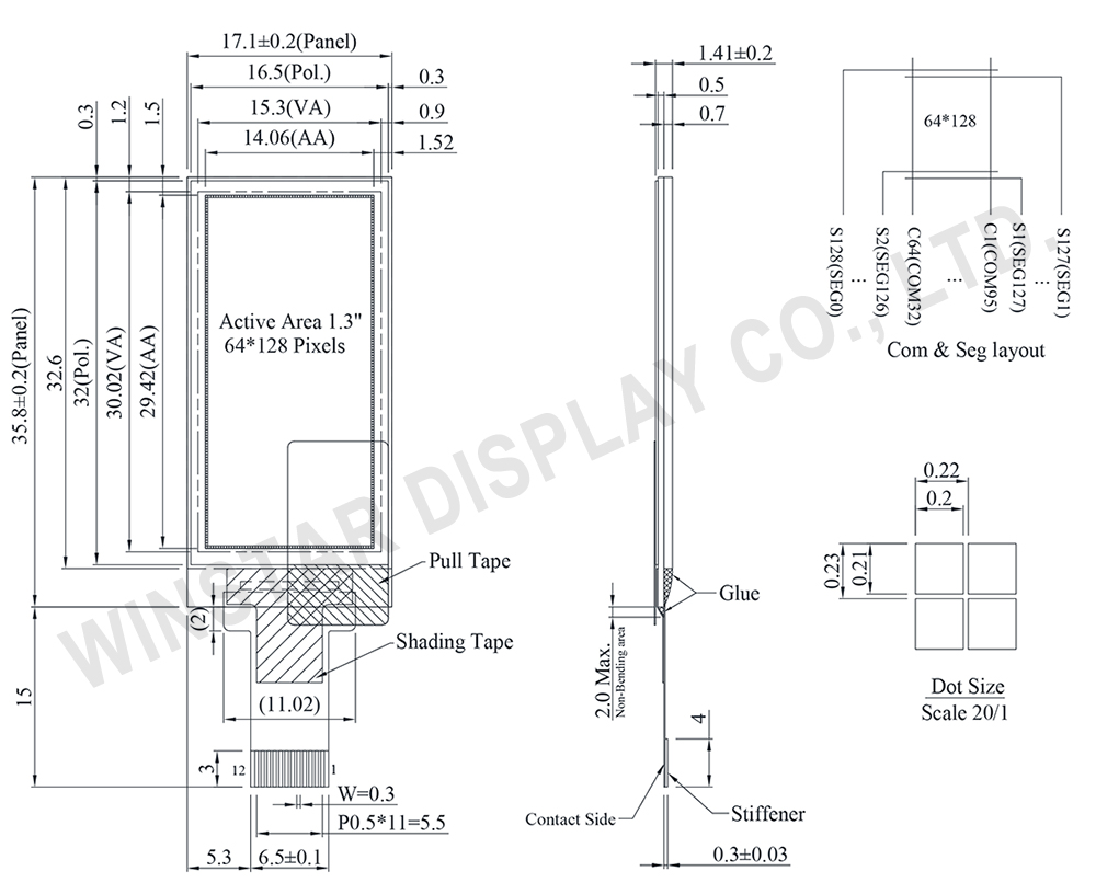
| 点阵(分辨率) | 64 x 128 | Dots |
| 模块尺寸 | 17.1 × 35.80 × 1.41 | mm |
| 有效区域 | 14.06 × 29.42 | mm |
| 像素大小 | 0.20 × 0.21 | mm |
| 像素间距 | 0.22 × 0.23 | mm |
| 显示模式 | 被动矩阵 | |
| 发光颜色 | 单色 | |
| 驱动方式 | 1/64 Duty | |
| IC | SH1107 | |
| 界面 | 4-线 SPI , I2C | |
| 尺寸 | 1.3 寸 | |
| 参数 | 符号 | 最小值 | 最大值 | 单位 |
|---|---|---|---|---|
| 逻辑电源电压 | VDD | -0.3 | 3.6 | V |
| 显示电源电压 | VPP | 7.0 | 17.0 | V |
| 工作温度 | TOP | -40 | +80 | °C |
| 储存温度 | TSTG | -40 | +85 | °C |
| 项目 | 符号 | 条件 | 最小值 | 典型值 | 最大值 | 单位 |
|---|---|---|---|---|---|---|
| 逻辑电源电压 | VDD | - | 1.65 | 3.0 | 3.5 | V |
| 显示电源电压 | VPP | - | 7.0 | 13.0 | 13.5 | V |
| 输入高电压 | VIH | - | 0.8×VDD | - | VDD | V |
| 输入低电压 | VIL | - | VSS | - | 0.2×VDD | V |
| 输出高电压 | VOH | - | 0.8×VDD | - | VDD | V |
| 输出低电压 | VOL | - | VSS | - | 0.2×VDD | V |
| 50% 开启显示 | IPP | VPP=13V | - | 10 | 15 | mA |
| No. | 符号 | 说明 |
|---|---|---|
| 1 | VSS | Ground. |
| 2 | D1 | When the serial interface is selected, then D0 serves as the serial clock input pad (SCL) and D1 serves as the serial data input pad (SI). When the I2C interface is selected, then D0 serves as the serial clock input pad (SCL) and D1 serves as the serial data input pad (SDA). |
| 3 | D0 | |
| 4 | A0 | This is the Data/Command control pad that determines whether the data bits are data or a command. A0 = “H”: Data. A0 = “L”: Command In I2C interface, this pad serves as SA0 to distinguish the different address of OLED driver. |
| 5 | ___ RES |
This is a reset signal input pad. When RES is set to “L”, the settings are initialized. The reset operation is performed by the RES signal level. |
| 6 | __ CS |
This pad is the chip select input. When CS = “L”, then the chip select becomes active, and data/command I/O is enabled. |
| 7 | IREF | This is a segment current reference pad. A resistor should be connected between this pad and VSS. Set the current at 15.625uA. |
| 8 | IM1 | These are the MPU interface mode select pads. IM1 connect to VDD is I2C interface. IM1 connect to VSS is 4-wire SPI interface. |
| 9 | VDD | Power supply for logic and input. |
| 10 | VCOMH | This is a pad for the voltage output high level for common signals. A capacitor should be connected between this pad and VSS. |
| 11 | VPP | This is the most positive voltage supply pad of the chip. It should be supplied externally. |
| 12 | VSS | Ground. |

通过点击「允许所有 Cookie」,代表您同意在您的设备上存储 Cookie 以增强网站浏览体验、分析网站使用情况并协助我们的营销和网站效能优化工作。您可以在我们的隐私权政策中找到有关于此的更多信息。