私たちはあなたのプライバシーを大切にします
「すべてのクッキーを許可」をクリックすると、サイトのナビゲーションを向上させ、サイト使用状況を分析し、マーケティングおよびパフォーマンスの取り組みを支援するために、クッキーをデバイスに保存することに同意したことになります。この件に関する詳細情報は、ポリシーをご覧ください。プライバシーポリシー


| Pin | 記号 | 説明 |
|---|---|---|
| 1 | CSB | Chip select input pin.Interface access is enabled when CSB is “L”,When CSB is non-active(CSB=”H”),D[7:0] pins are high impedance. |
| 2 | RSTB | Hardware reset input pin. When RSTB is “L”, interna initialization is executed and the internal registers will be initialized. |
| 3 | A0 | It determines whether the access is related to data or command. A0=“H” : Indicates that signals on D[7:0] are display data. A0=“L” : Indicates that signals on D[7:0] are command |
| 4 | RWR | Read/Write execution control pin. When PSB is “H”, RWR is not used in serial interface and should fix to “H” by VDD1 or VDDH. |
| 5 | ERD | Read/Write execution control pin. When PSB is “H”, ERD is not used in serial interface and should fix to “H” by VDD1 or VDDH. |
| 6 | D0 | When using 8-bit parallel interface: (6800 or 8080 mode) 8-bit bi-directional data bus. Connect to the data bus of 8-bit microprocessor. When CSB is non-active (CSB=“H”), D[7:0] pins are high impedance. |
| 7 | D1 | |
| 8 | D2 | |
| 9 | D3 | |
| 10 | D4 | |
| 11 | D5 | |
| 12 | D6 | |
| 13 | D7 | |
| 14 | VDD | Power supply |
| 15 | Vss | Ground |
| 16-19 | NC | Not connect. |
| 20 | V0 | V0 is the LCD driving voltage for common circuits at negative frame. |
| 21 | XV0 | XV0 is the LCD driving voltage for common circuits at positive frame. |
| 22 | VG | VG is the LCD driving voltage for segment circuits. |
| 23-27 | NC | Not connect. |
| 28 | C86 | C86 selects the microprocessor type in parallel interface mode. |
| 29 | PSB | PSB selects the interface type: Serial or Parallel. |
| 30 | NC | Not connect. |
| 項目 | 仕様 | 単位 |
|---|---|---|
| ドットマトリックス(解像度) | 128 x 64 | - |
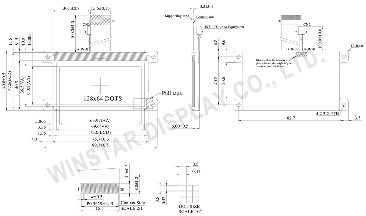
| モジュールサイズ | 89.7 x 49.8 x 6.0 | mm |
| 表示エリア | 69.0 x 36.5 | mm |
| 有効エリア | 63.97 x 31.97 | mm |
| ドットサイズ | 0.47 x 0.47 | mm |
| ドットピッチ | 0.5 x 0.5 | mm |
| 駆動方法 | 1/65 , 1/9 Bias | |
| バックライトタイプ | LED | |
| IC | ST7567 | |
| インターフェイス | 6800/8080/4-Line SPI | |
| 項目 | 記号 | 最小値 | 典型値 | 最大値 | 単位 |
|---|---|---|---|---|---|
| 操作温度 | TOP | -20 | - | +70 | ℃ |
| 保存温度 | TST | -30 | - | +80 | ℃ |
| 入力電圧 | VI | -0.3 | - | VDD+0.3 | V |
| デジタル電源電圧 | VDD-Vss | -0.3 | - | 3.6 | V |
| 電源電圧 | V0-XV0 | -0.3 | - | 16 | V |
| 項目 | 記号 | 条件 | 最小値 | 典型値 | 最大値 | 単位 |
|---|---|---|---|---|---|---|
| ロジック電源電圧 | VDD-VSS | - | 2.8 | 3.0 | 3.2 | V |
| LCD供給電圧 | VOP | Ta=-20℃ Ta=25℃ Ta=70℃ |
- 9.3 - |
- 9.5 - |
- 9.7 - |
V V V |
| 高レベル入力電圧 | VIH | - | 0.7 VDD | - | VDD | V |
| 低レベル入力電圧 | VIL | - | Vss | - | 0.3VDD | V |
| 高レベル出力電圧 | VOH | - | 0.8 VDD | - | VDD | V |
| 低レベル出力電圧 | VOL | - | Vss | - | 0.2VDD | V |
| 供給電流 | IDD | VDD=3.0V | - | 0.7 | 1.0 | mA |
Search Keyword: lcd 128x64, lcd 128 x 64, 128x64 lcd, 128 x 64 lcd

「すべてのクッキーを許可」をクリックすると、サイトのナビゲーションを向上させ、サイト使用状況を分析し、マーケティングおよびパフォーマンスの取り組みを支援するために、クッキーをデバイスに保存することに同意したことになります。この件に関する詳細情報は、ポリシーをご覧ください。プライバシーポリシー