 - WG12232E")
我們重視您的隱私
通過點擊「允許所有 Cookie」,代表您同意在您的設備上存儲 Cookie 以增強網站瀏覽體驗、分析網站使用情況並協助我們的行銷和網站效能優化工作。您可以在我們的隱私權政策中找到有關於此的更多資訊。

 - WEO012832R")
 - WEO012832R")
 - WEO012832R")
 - WEO012832R")
 - WEO012832R")
 - WEO012832R")
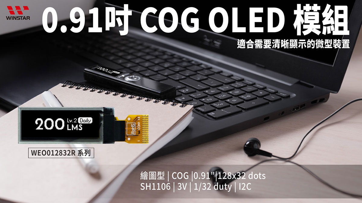
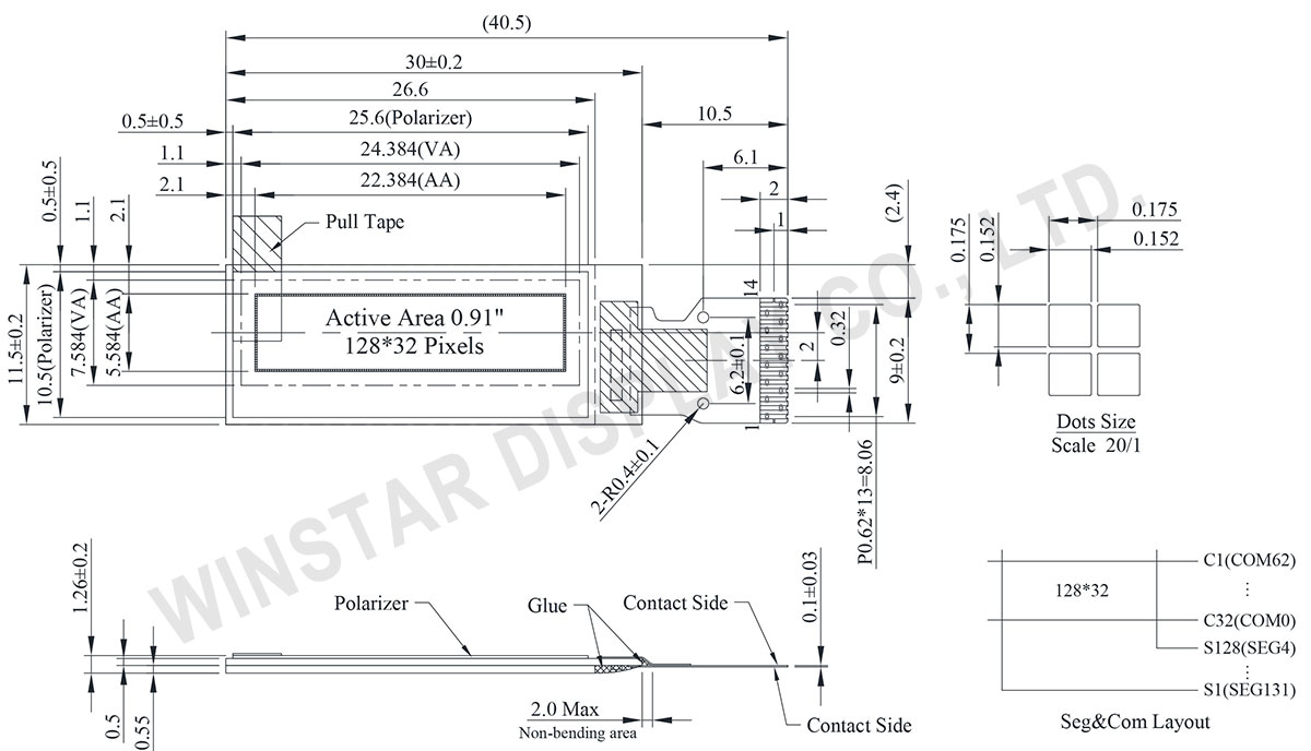
WEO012832R 系列是市場上相當受歡迎的 0.91 吋 COG 繪圖型 I2C OLED 模組。此模組有 128x32 dots 的解析度,並整合了支援 I2C 介面的 SH1106 IC。此 IC 可提供內部升壓及外部供電。模組的外形尺寸為 30.0 × 11.5 mm,有效顯示區域為 22.384 × 5.584 mm,由於採用 COG 結構,厚度僅有 1.26 mm,非常輕巧。
邏輯電源供應電壓範圍從 1.65V ~ 3.3V,典型值為 3.0V,驅動方式 1/32 duty。此外,模組具有廣泛的溫度範圍,能可靠的工作溫度範圍 -40℃ ~ +80℃,儲存溫度範圍 -40℃ ~ +85℃。
這款模組特別適用於需要輕巧 OLED 顯示器的各種應用。它非常適合整合到內嵌 OLED 顯示器的錄音筆、充電傳輸線和配備OLED 顯示器的鑰匙扣燈...等產品中,特別是在空間和視覺清晰度要求較高的場合。
Data source ref:WEO012832RSPP3N00000
| 項目 | 規格 | 單位 |
|---|---|---|
| 點陣(解析度) | 128 × 32 | Dots |
| 模組尺寸 | 30.0 × 11.5 × 1.26 | mm |
| 有效區域 | 22.384 × 5.584 | mm |
| 像素大小 | 0.152 × 0.152 | mm |
| 像素間距 | 0.175 × 0.175 | mm |
| 顯示模式 | Passive Matrix 被動矩陣 | |
| 發光顏色 | 單色 | |
| 驅動方式 | 1/32 Duty | |
| IC | SH1106 | |
| 介面 | I2C | |
| 尺寸(對角線) | 0.91吋 | |
| 參數 | 符號 | 最小值 | 最大值 | 單位 |
|---|---|---|---|---|
| 邏輯電源電壓 | VDD1 | -0.3 | 3.6 | V |
| 充電泵電路的電源供應 | VDD2 | -0.3 | 4.8 | V |
| 顯示電源電壓 | VPP | -0.3 | 14.5 | V |
| 工作溫度 | TOP | -40 | +80 | °C |
| 儲存溫度 | TSTG | -40 | +85 | °C |
| 項目 | 符號 | 條件 | 最小值 | 典型值 | 最大值 | 單位 |
|---|---|---|---|---|---|---|
| 邏輯電源電壓 | VDD1 | - | 1.65 | 3.0 | 3.3 | V |
| 顯示電源電壓 (外部供應) | VPP | - | 6.4 | 7.25 | 8 | V |
| 充電泵穩壓器的供應電壓 | VDD2 | - | 2.9 | - | 4.2 | V |
| 顯示器的充電泵輸出電壓 (Generated by Internal DC/DC) | Charge Pump VPP |
- | 7.0 | 7.4 | - | V |
| 輸入高準位 | VIH | - | 0.8×VDD1 | - | VDD1 | V |
| 輸入低準位 | VIL | - | VSS | - | 0.2×VDD1 | V |
| 輸出高準位 | VOH | - | 0.8×VDD1 | - | VDD1 | V |
| 輸出低準位 | VOL | - | VSS | - | 0.2×VDD1 | V |
| VPP(外部供應的VPP)的操作電流 | IPP | VPP =7.25V | - | 8 | 12 | mA |
| 顯示器50%像素開啟時(由內部DC/DC產生的VPP) | IDD2 | - | - | 15 | 25 | mA |
| No. | 符號 | 功能說明 |
|---|---|---|
| 1 | C1N | Connect to charge pump capacitor. These pins are not used and should be disconnected when Vpp is supplied externally. |
| 2 | C1P | |
| 3 | C2P | |
| 4 | C2N | |
| 5 | VDD2 | Power supply pad for Power supply for charge pump circuit. This pin should be disconnected when VPP is supplied externally |
| 6 | NC | No connection |
| 7 | VSS | Ground. |
| 8 | VDD1 | Power supply input |
| 9 | RES# | This is a reset signal input pad. When RES is set to “L”, the settings are initialized. The reset operation is performed by the RES signal level. |
| 10 | SCL | When the I2C interface is selected, D0 serves as the serial clock input pad (SCL) and D1 serves as the serial data input pad (SDAI). |
| 11 | SDA | |
| 12 | IREF | This is a segment current reference pad. A resistor should be connected between this pad and VSS. Set the current at 18.75uA. |
| 13 | VCOMH | This is a pad for the voltage output high level for common signals. A capacitor should be connected between this pad and VSS. |
| 14 | VPP | OLED panel power supply. Generated by internal charge pump. Connect to capacitor. It could be supplied externally. |

通過點擊「允許所有 Cookie」,代表您同意在您的設備上存儲 Cookie 以增強網站瀏覽體驗、分析網站使用情況並協助我們的行銷和網站效能優化工作。您可以在我們的隱私權政策中找到有關於此的更多資訊。