
我们重视您的隐私
通过点击「允许所有 Cookie」,代表您同意在您的设备上存储 Cookie 以增强网站浏览体验、分析网站使用情况并协助我们的营销和网站效能优化工作。您可以在我们的隐私权政策中找到有关于此的更多信息。
 - WEO002002A")
 - WEO002002A")
 - WEO002002A")
20字x2行 COG 字符 OLED 显示器模块(型号:WEO002002A)采用 COG(Chip On Glass)结构设计,提供高性能且可靠的显示解决方案。这款 OLED 模块因其卓越的显示效果和出色的耐用性,已在多种应用中得到广泛应用。
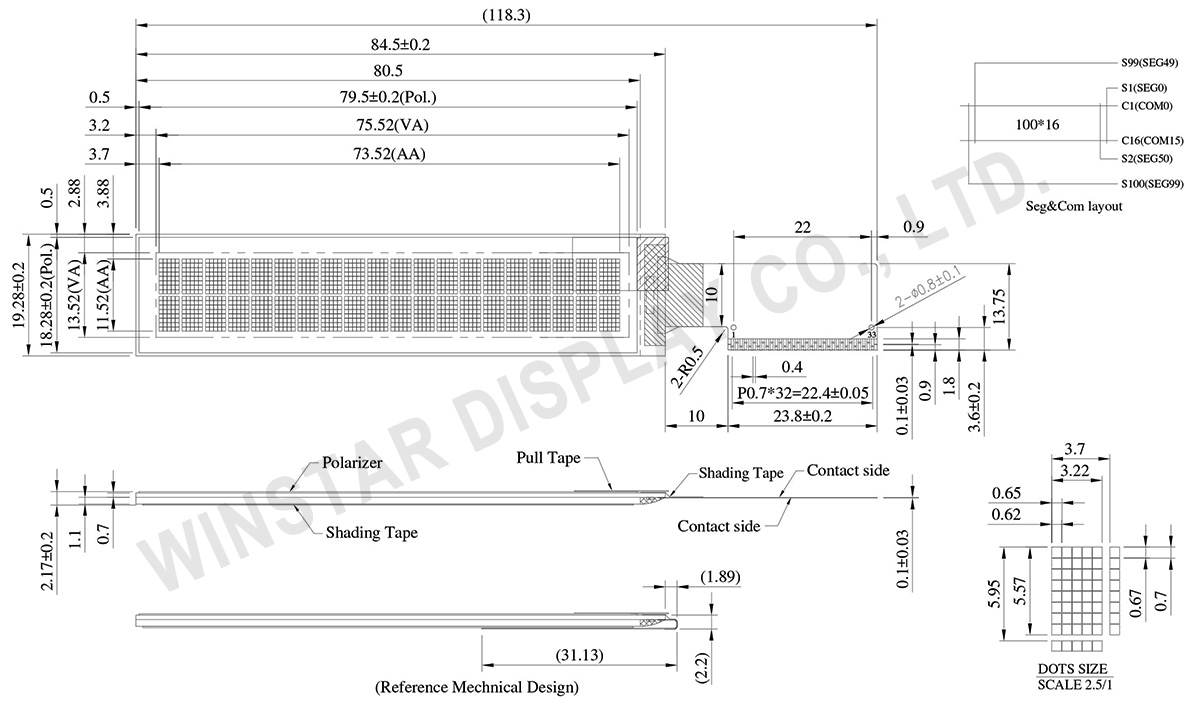
WEO002002A模块的外型尺寸为 84.5 x 19.28 mm,厚度为 2.17 mm,显示区域的有效尺寸为 73.52 x 11.52 mm,对角线尺寸为 2.93 寸。模块配备 SSD1311 驱动 IC,支持内建字库,能够显示包括 ASCII、英文、欧文和日文在内的多种文字集。每个字符由 5x8 像素组成,确保显示效果细致且清晰。
此模块的显示模式为 2 行,每行可显示 20 个字符。由于 OLED 技术的自发光特性,此模块无需背光,这不仅使其设计更加轻薄,还提升了显示对比度,达到 10,000:1。模块还具备超广视角(高达 175 度),确保从不同角度观察时显示效果的一致性。此外,它还具有低功耗和广泛的工作温度范围,显示其卓越的适应性。
WEO002002A 的工作温度范围为 -40°C 至 +80°C,储存温度范围为 -40°C 至 +85°C,能够在各种极端环境下稳定运行。模块的逻辑电压范围为 2.4V 至 3.3V,典型值为 3V,并采用 1/16 duty 驱动方式。
此外,WEO002002A 支持多种接口选择,包括 6800/8080并列接口、SPI/I2C 串行接口,提供灵活的连接选择以满足不同系统的需求。该型号系列还提供多种软性印刷电路板(Flexible Printed Circuit, FPC)选择,以满足客户的各种需求。
WEO002002A OLED 显示器模块以其卓越的显示质量、广泛的工作温度范围和灵活的接口选择,成为取代传统 LCD 模块的理想选择。我们建议客户考虑使用这款 20x2 字符 OLED 模块,以提升产品的显示性能,实现更高的显示质量和更低的能耗。
 可选 FPC
| 项目 | 尺寸 | 单位 |
|---|---|---|
| 字符数 | 20字x2行 | - |
| 模块尺寸 | 84.5 x 19.28 x 2.17 | mm |
| 检视区域 | 75.52 x 13.52 | mm |
| 有效区域 | 73.52 x 11.52 | mm |
| 点大小 | 0.62 x 0.67 | mm |
| 点间距 | 0.65 x 0.70 | mm |
| 字符尺寸 | 3.22 x 5.57 | mm |
| 字符间距 | 3.70 x 5.95 | mm |
| LCD类型 | OLED , 单色 | |
| Duty | 1/16 | |
| IC | SSD1311 | |
| 接口 | 6800, 8080, SPI, I2C | |
| 尺寸 | 2.93 寸 | |
| 项目 | 符号 | 最小值 | 最大值 | 单位 |
|---|---|---|---|---|
| 逻辑电源电压 | VDD | -0.3 | VDDIO | V |
| 输入/输出针脚(Pin)电源 | VDDIO | -0.3 | 6 | V |
| 工作电压 | VCC | 0 | 16 | V |
| 工作温度 | TOP | -40 | +80 | ℃ |
| 储存温度 | TST | -40 | +85 | ℃ |
| 项目 | 符号 | 条件 | 最小值 | 典型值 | 最大值 | 单位 |
|---|---|---|---|---|---|---|
| 逻辑电源电压 | VDD | Low Voltage I/O | 2.4 | 3.0 | 3.3 | V |
| 5V I/O (VDD as output) |
- | - | - | V | ||
| 输入/输出针脚(Pin)电源 | VDDIO | Low Voltage I/O | 2.4 | 3.0 | 3.3 | V |
| 5V I/O | 4.4 | 5.0 | 5.3 | V | ||
| 工作电压 | VCC | - | 8.0 | 10.0 | 10.5 | V |
| - | 8.0 | 12.0 | 12.5 | V | ||
| 输入高电压 | VIH | - | 0.8xVDDIO | - | - | V |
| 输入低电压 | VIL | - | - | - | 0.2xVDDIO | V |
| 输出高电压 | VOH | IOH=-0.5mA | 0.9xVDDIO | - | - | V |
| 输出低电压 | VOL | IOL=0.5mA | - | - | 0.1xVDDIO | V |
| 50%显示画面耗电流 | ICC | VCC=10V | - | 18 | 27 | mA |
| VCC=12V | - | 25 | 38 | mA |
| Pin No. | 符号 | Pin 类型 | 说明 | ||||||||||||||||||||
|---|---|---|---|---|---|---|---|---|---|---|---|---|---|---|---|---|---|---|---|---|---|---|---|
| 1 | NC | - | No connection | ||||||||||||||||||||
| 2 | VSL | P | This is segment voltage (output low level) reference pin. When external VSL is not used, this pin should be left open. When external VSL is used, connect with resistor and diode to ground (details depend on application). |
||||||||||||||||||||
| 3 | VSS | P | Ground pin. It must be connected to external ground. | ||||||||||||||||||||
| 4 | REGVDD | I | Internal VDD regulator selection pin in 5V I/O application mode. When this pin is pulled HIGH, internal VDD regulator is enabled (5V I/O application). When this pin is pulled LOW, internal VDD regulator is disabled (Low voltage I/O application). |
||||||||||||||||||||
| 5 | SHLC | I |
This pin is used to determine the Common output scanning direction.
(1) 0 is connected to VSS (2) 1 is connected to VDDIO
|
||||||||||||||||||||
| 6 | SHLS | I | This pin is used to change the mapping between the display data column address and the Segment driver. SEG scan direction
(1) 0 is connected to VSS (2) 1 is connected to VDDIO |
||||||||||||||||||||
| 7 | VDD | P | Power supply for core logic operation. VDD can be supplied externally or regulated internally. In LV IO application (internal VDD is disabled), this is a power input pin. In 5V IO application (internal VDD is enabled), VDD is regulated internally from VDDIO. A capacitor should be connected between VDD and VSS under all circumstances. |
||||||||||||||||||||
| 8 | VDDIO | P | Low voltage power supply and power supply for interface logic level in both Low Voltage I/O and 5V I/O application. It should match with the MCU interface voltage level and must be connected to external source. | ||||||||||||||||||||
| 9 | BS0 | I | MCU bus interface selection pins. Select appropriate logic setting as described in the following table. BS2, BS1 and BS0 are pin select. Bus Interface selection
(1) 0 is connected to VSS (2) 1 is connected to VDDIO |
||||||||||||||||||||
| 10 | BS1 | ||||||||||||||||||||||
| 11 | BS2 | ||||||||||||||||||||||
| 12 | GPIO | I/O | It is a GPIO pin. Details refer to OLED command DCh. | ||||||||||||||||||||
| 13 | CS# | I | This pin is the chip select input connecting to the MCU. The chip is enabled for MCU communication only when CS# is pulled LOW (active LOW). In I2C mode, this pin must be connected to VSS. |
||||||||||||||||||||
| 14 | RES# | I | This pin is reset signal input. When the pin is pulled LOW, initialization of the chip is executed. Keep this pin pull HIGH during normal operation. |
||||||||||||||||||||
| 15 | D/C# | I | This pin is Data/Command control pin connecting to the MCU. When the pin is pulled HIGH, the data at D[7:0] will be interpreted as data. When the pin is pulled LOW, the data at D[7:0] will be transferred to a command register. In I2C mode, this pin acts as SA0 for slave address selection. When serial interface is selected, this pin must be connected to VSS. |
||||||||||||||||||||
| 16 | R/W#(WR#) | I | This pin is read / write control input pin connecting to the MCU interface. When 6800 interface mode is selected, this pin will be used as Read/Write (R/W#) selection input. Read mode will be carried out when this pin is pulled HIGH and write mode when LOW. When 8080 interface mode is selected, this pin will be the Write (WR#) input. Data write operation is initiated when this pin is pulled LOW and the chip is selected. When serial or I2C interface is selected, this pin must be connected to VSS. |
||||||||||||||||||||
| 17 | E(RD#) | I | This pin is MCU interface input. When 6800 interface mode is selected, this pin will be used as the Enable (E) signal. Read/write operation is initiated when this pin is pulled HIGH and the chip is selected. When 8080 interface mode is selected, this pin receives the Read (RD#) signal. Read operation is initiated when this pin is pulled LOW and the chip is selected. When serial or I2C interface is selected, this pin must be connected to VSS. |
||||||||||||||||||||
| 18 | D0 | I/O | These pins are bi-directional data bus connecting to the MCU data bus. Unused pins are recommended to tie LOW. When serial interface mode is selected, D0 will be the serial clock input: SCLK; D1 will be the serial data input: SID and D2 will be the serial data output: SOD. When I2C mode is selected, D2, D1 should be tied together and serve as SDAout, SDAin in application and D0 is the serial clock input, SCL. |
||||||||||||||||||||
| 19 | D1 | ||||||||||||||||||||||
| 20 | D2 | ||||||||||||||||||||||
| 21 | D3 | ||||||||||||||||||||||
| 22 | D4 | ||||||||||||||||||||||
| 23 | D5 | ||||||||||||||||||||||
| 24 | D6 | ||||||||||||||||||||||
| 25 | D7 | ||||||||||||||||||||||
| 26 | IREF | I | This pin is the segment output current reference pin. IREF is supplied externally. A resistor should be connected between this pin and VSS to maintain current of around 15uA. |
||||||||||||||||||||
| 27 | ROM0 | I | These pins are used to select Character ROM; select appropriate logic setting as described in the following table. ROM1 and ROM0 are pin select as shown in below table: Character ROM selection
(1) 0 is connected to VSS (2) 1 is connected to VDDIO |
||||||||||||||||||||
| 28 | ROM1 | ||||||||||||||||||||||
| 29 | OPR0 | I | This pin is used to select the character number of character generator. Character RAM selection
(1) 0 is connected to VSS (2) 1 is connected to VDDIO |
||||||||||||||||||||
| 30 | OPR1 | ||||||||||||||||||||||
| 31 | VCOMH | P | COM signal deselected voltage level. A capacitor should be connected between this pin and VSS. No external power supply is allowed to connect to this pin. |
||||||||||||||||||||
| 32 | VCC | P | Power supply for panel driving voltage. This is also the most positive power voltage supply pin. It is supplied by external high voltage source. | ||||||||||||||||||||
| 33 | NC | - | No connection |
| 图示 | FPC 全长 | PIN | pitch | ZIF FPC 或 HOTBAR FPC | 界面 | FPC No. | 建立日期 |
|---|---|---|---|---|---|---|---|
 |
34.9 | 31 | 0.7 | HOTBAR FPC | 6800, 8080, SPI, I2C | FPC2070003111XXXXX01 | 20160817 |
 |
31 | 31 | 0.5 | ZIF FPC | 6800, 8080, SPI, I2C | FPC2005003421XXXXX00 | 20180313 |
Search keyword: oled 20x2, 20x2 oled

通过点击「允许所有 Cookie」,代表您同意在您的设备上存储 Cookie 以增强网站浏览体验、分析网站使用情况并协助我们的营销和网站效能优化工作。您可以在我们的隐私权政策中找到有关于此的更多信息。