
우리는 귀하의 프라이버시를 소중히 여깁니다
"모든 쿠키 허용"을 클릭하면 사이트 탐색을 개선하고, 사이트 사용을 분석하며, 마케팅 및 성능 노력에 도움을 주기 위해 쿠키를 귀하의 장치에 저장하는 데 동의한 것으로 간주됩니다. 이 주제에 대한 추가 정보는 당사의 정책에서 확인할 수 있습니다. 개인정보 보호정책


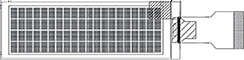
20x4 COG SSD1311 OLED 디스플레이 모듈 (모델: WEO002004C)은 COG(Chip On Glass) 설계를 채택하여 높은 성능과 신뢰성을 제공하는 디스플레이 솔루션을 제공합니다. 이 SSD1311 OLED 디스플레이 모듈은 우수한 디스플레이 품질과 내구성으로 다양한 응용 분야에 적합합니다.
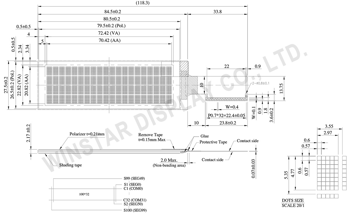
모듈의 크기는 84.5 x 27.5 mm, 두께는 2.17 mm이며, 유효 표시 영역은 70.42 x 20.82 mm, 대각선 크기는 2.89인치입니다. SSD1311 드라이버 IC가 탑재된 WEO002004C는 ASCII, 영어, 유럽 언어 및 일본어를 포함하는 통합 문자 세트를 지원합니다. 각 문자는 5x8 픽셀로 구성되어 있어 세밀하고 선명한 텍스트 표현이 가능합니다.
이 모듈의 디스플레이 모드는 4행이며, 각 행에 20자를 표시할 수 있습니다. OLED 기술의 자가 발광 특성으로 인해 백라이트가 필요 없으며, 이로 인해 더 가볍고 얇은 디자인이 가능해지고, 대비 비율은 10,000:1로 향상됩니다. 또한 최대 175도의 초광시야각을 제공하여 다양한 각도에서 일관된 디스플레이 품질을 보장합니다. 모듈은 낮은 전력 소모와 넓은 작동 온도 범위를 제공하여 뛰어난 적응성을 자랑합니다.
WEO002004C의 작동 온도 범위는 -40°C에서 +80°C까지이며, 저장 온도 범위는 -40°C에서 +85°C까지로 극한의 조건에서도 안정적인 성능을 발휘합니다. 모듈은 2.4V에서 3.3V의 논리 전압 범위 내에서 작동하며, 전형적인 값은 3V, 1/32 듀티 구동 방식을 채택하고 있습니다.
또한, WEO002004C는 6800/8080 8비트 병렬 및 I2C/SPI 시리얼 인터페이스를 포함한 다양한 인터페이스 옵션을 지원하여 다양한 시스템 요구 사항에 맞는 유연한 연결성을 제공합니다. 이 모듈 시리즈는 고객의 다양한 요구에 맞춘 여러 가지 플렉시블 프린트 회로(FPC) 옵션도 제공합니다.
신뢰할 수 있는 디스플레이 품질, 넓은 작동 온도 범위 및 유연한 인터페이스 옵션을 갖춘 WEO002004C OLED 디스플레이 모듈은 기존 LCD 모듈에 대한 실용적인 대안입니다. 이 20x4 문자 OLED 모듈을 사용하여 제품의 디스플레이 성능을 향상시키고, 뛰어난 디스플레이 품질과 낮은 전력 소모를 달성하는 것을 권장합니다.
 FPC 옵션
| 항목 | 치수 | 단위 |
|---|---|---|
| 디스플레이 형식 | 20 문자 x 4 라인 | - |
| 모듈 치수 | 84.5 x 27.5 x 2.17 | mm |
| 보기 영역 | 72.42 x 22.82 | mm |
| 활성 영역 | 70.42 x 20.82 | mm |
| 도트 크기 | 0.57 x 0.57 | mm |
| 도트 피치 | 0.60 x 0.60 | mm |
| 캐릭터 크기 | 2.97 x 4.77 | mm |
| 캐릭터 피치 | 3.55 x 5.35 | mm |
| LCD 유형 | OLED , Monochrome | |
| Duty | 1/32 | |
| IC | SSD1311 | |
| 인터페이스 | 6800,8080,SPI,I2C | |
| 크기 (대각선) | 2.89 인치 | |
| 항목 | 기호 | 최소값 | 최대값 | 단위 |
|---|---|---|---|---|
| Supply Voltage For Logic | VDD | -0.3 | VDDIO | V |
| Power Supply for I/O pins | VDDIO | -0.3 | 6 | V |
| Operating Voltage | VCC | 0 | 16 | V |
| 작동 온도 | TOP | -40 | +80 | °C |
| 보관 온도 | TST | -40 | +85 | °C |
| 항목 | 기호 | 조건 | 최소값 | 대표값 | 최대값 | 단위 |
|---|---|---|---|---|---|---|
| Supply Voltage For Logic | VDD | Low Voltage I/O | 2.4 | 3.0 | 3.3 | V |
| 5V I/O (VDD as output) |
- | - | - | V | ||
| Power supply for I/O pins | VDDIO | Low Voltage I/O | 2.4 | 3.0 | 3.3 | V |
| 5V I/O | 4.4 | 5.0 | 5.3 | V | ||
| Operating Voltage | VCC | - | 8.0 | 10.0 | 10.5 | V |
| 8.0 | 12.0 | 12.5 | V | |||
| Input High Volt. | VIH | - | 0.8xVDDIO | - | - | V |
| Input Low Volt. | VIL | - | - | - | 0.2xVDDIO | V |
| Output High Volt. | VOH | IOH=-0.5mA | 0.9xVDDIO | - | - | V |
| Output Low Volt. | VOL | IOL=0.5mA | - | - | 0.1xVDDIO | V |
| 50% Check Board Operating Current | ICC | VCC=10V | - | 19 | 29 | mA |
| VCC=12V | - | 23 | 35 | mA |
| Pin No. | 기호 | Pin Type | 기능 | ||||||||||||||||||||
|---|---|---|---|---|---|---|---|---|---|---|---|---|---|---|---|---|---|---|---|---|---|---|---|
| 1 | NC | - | No connection | ||||||||||||||||||||
| 2 | VSL | P | This is segment voltage (output low level) reference pin. When external VSL is not used, this pin should be left open. When external VSL is used, connect with resistor and diode to ground (details depend on application). |
||||||||||||||||||||
| 3 | VSS | P | Ground pin. It must be connected to external ground. | ||||||||||||||||||||
| 4 | REGVDD | I | Internal VDD regulator selection pin in 5V I/O application mode. When this pin is pulled HIGH, internal VDD regulator is enabled (5V I/O application). When this pin is pulled LOW, internal VDD regulator is disabled (Low voltage I/O application). |
||||||||||||||||||||
| 5 | SHLC | I | This pin is used to determine the Common output scanning direction. COM scan direction
(1) 0 is connected to VSS (2) 1 is connected to VDDIO |
||||||||||||||||||||
| 6 | SHLS | I | This pin is used to change the mapping between the display data column address and the Segment driver. SEG scan direction
(1) 0 is connected to VSS (2) 1 is connected to VDDIO |
||||||||||||||||||||
| 7 | VDD | P | Power supply for core logic operation. VDD can be supplied externally or regulated internally. In LV IO application (internal VDD is disabled), this is a power input pin. In 5V IO application (internal VDD is enabled), VDD is regulated internally from VDDIO. A capacitor should be connected between VDD and VSS under all circumstances. |
||||||||||||||||||||
| 8 | VDDIO | P | Low voltage power supply and power supply for interface logic level in both Low Voltage I/O and 5V I/O application. It should match with the MCU interface voltage level and must be connected to external source. | ||||||||||||||||||||
| 9 | BS0 | I | MCU bus interface selection pins. Select appropriate logic setting as described in the following table. BS2, BS1 and BS0 are pin select. Bus Interface selection
(1) 0 is connected to VSS (2) 1 is connected to VDDIO |
||||||||||||||||||||
| 10 | BS1 | ||||||||||||||||||||||
| 11 | BS2 | ||||||||||||||||||||||
| 12 | GPIO | I/O | It is a GPIO pin. Details refer to OLED command DCh. | ||||||||||||||||||||
| 13 | CS# | I | This pin is the chip select input connecting to the MCU. The chip is enabled for MCU communication only when CS# is pulled LOW (active LOW). In I2C mode, this pin must be connected to VSS. |
||||||||||||||||||||
| 14 | RES# | I | This pin is reset signal input. When the pin is pulled LOW, initialization of the chip is executed. Keep this pin pull HIGH during normal operation. |
||||||||||||||||||||
| 15 | D/C# | I | This pin is Data/Command control pin connecting to the MCU. When the pin is pulled HIGH, the data at D[7:0] will be interpreted as data. When the pin is pulled LOW, the data at D[7:0] will be transferred to a command register. In I2C mode, this pin acts as SA0 for slave address selection. When serial interface is selected, this pin must be connected to VSS. |
||||||||||||||||||||
| 16 | R/W#(WR#) | I | This pin is read / write control input pin connecting to the MCU interface. When 6800 interface mode is selected, this pin will be used as Read/Write (R/W#) selection input. Read mode will be carried out when this pin is pulled HIGH and write mode when LOW. When 8080 interface mode is selected, this pin will be the Write (WR#) input. Data write operation is initiated when this pin is pulled LOW and the chip is selected. When serial or I2C interface is selected, this pin must be connected to VSS. |
||||||||||||||||||||
| 17 | E(RD#) | I | This pin is MCU interface input. When 6800 interface mode is selected, this pin will be used as the Enable (E) signal. Read/write operation is initiated when this pin is pulled HIGH and the chip is selected. When 8080 interface mode is selected, this pin receives the Read (RD#) signal. Read operation is initiated when this pin is pulled LOW and the chip is selected. When serial or I2C interface is selected, this pin must be connected to VSS. |
||||||||||||||||||||
| 18 | D0 | I/O | These pins are bi-directional data bus connecting to the MCU data bus. Unused pins are recommended to tie LOW. When serial interface mode is selected, D0 will be the serial clock input: SCLK; D1 will be the serial data input: SID and D2 will be the serial data output: SOD. When I2C mode is selected, D2, D1 should be tied together and serve as SDAout, SDAin in application and D0 is the serial clock input, SCL. |
||||||||||||||||||||
| 19 | D1 | ||||||||||||||||||||||
| 20 | D2 | ||||||||||||||||||||||
| 21 | D3 | ||||||||||||||||||||||
| 22 | D4 | ||||||||||||||||||||||
| 23 | D5 | ||||||||||||||||||||||
| 24 | D6 | ||||||||||||||||||||||
| 25 | D7 | ||||||||||||||||||||||
| 26 | IREF | I | This pin is the segment output current reference pin. IREF is supplied externally. A resistor should be connected between this pin and VSS to maintain current of around 15uA. |
||||||||||||||||||||
| 27 | ROM0 | I | These pins are used to select Character ROM; select appropriate logic setting as described in the following table. ROM1 and ROM0 are pin select as shown in below table: Character ROM selection
(1) 0 is connected to VSS (2) 1 is connected to VDDIO |
||||||||||||||||||||
| 28 | ROM1 | ||||||||||||||||||||||
| 29 | OPR0 | I | This pin is used to select the character number of character generator. Character RAM selection
Note (1) 0 is connected to VSS (2) 1 is connected to VDDIO |
||||||||||||||||||||
| 30 | OPR1 | ||||||||||||||||||||||
| 31 | VCOMH | P | COM signal deselected voltage level. A capacitor should be connected between this pin and VSS. No external power supply is allowed to connect to this pin. |
||||||||||||||||||||
| 32 | VCC | P | Power supply for panel driving voltage. This is also the most positive power voltage supply pin. It is supplied by external high voltage source. | ||||||||||||||||||||
| 33 | NC | - | No connection |
| 그림 | FPC Length | PIN | pitch | ZIF FPC or HOTBAR FPC | 인터페이스 | FPC No. | Create Date |
|---|---|---|---|---|---|---|---|
 |
35.2 | 31 | 0.7 | BOTBAR FPC | 6800,8080,SPI,I2C | FPC2070003111XXXXX00 | 20120921 |
 |
31 | 34 | 0.5 | ZIF FPC | 6800,8080,SPI,I2C | FPC2005003421XXXXX00 | 20151223 |
Search keyword: oled 20x4, 20x4 oled

"모든 쿠키 허용"을 클릭하면 사이트 탐색을 개선하고, 사이트 사용을 분석하며, 마케팅 및 성능 노력에 도움을 주기 위해 쿠키를 귀하의 장치에 저장하는 데 동의한 것으로 간주됩니다. 이 주제에 대한 추가 정보는 당사의 정책에서 확인할 수 있습니다. 개인정보 보호정책