Home Prodotti Display OLED Display OLED a Caratteri WEO002004C

Modulo OLED 20x4 COG SSD1311 da 2,89"

Modello numero WEO002004C

►Tipo : a caratteri
►Struttura : COG
►20 caratteri x 4 righe
►IC:SSD1311
►Alimentatore 3V/5V
►1/32 duty
►Interfaccia: 6800, 8080, SPI, I2C
►Colore display: Bianco / Giallo
►Altre opzioni FPC disponibili nella tabella di seguito

Descrizione

Il modulo OLED 20x4 COG SSD1311 (modello: WEO002004C) presenta un design COG (Chip On Glass), offrendo una soluzione di visualizzazione ad alte prestazioni e affidabile. Questo modulo OLED SSD1311 è rinomato per la sua eccellente qualità di visualizzazione e durata, rendendolo ideale per una varietà di applicazioni.

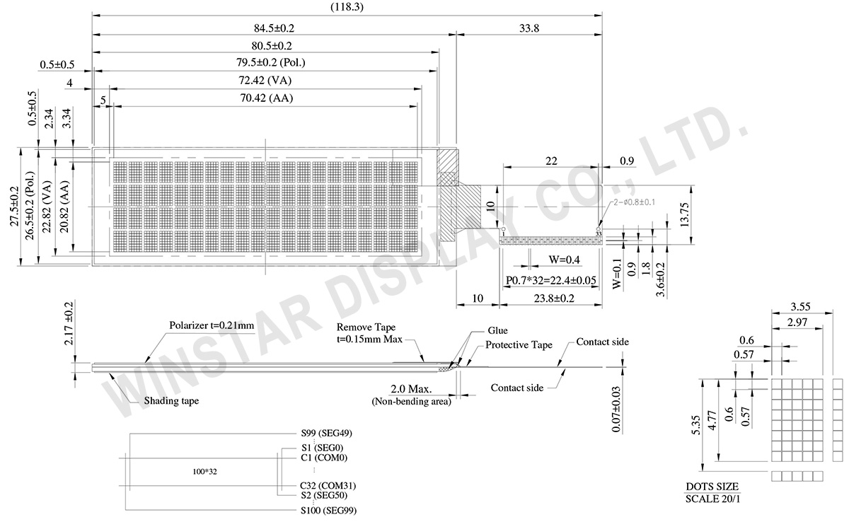
Le dimensioni del modulo sono 84,5 x 27,5 mm con uno spessore di 2,17 mm, e l'area attiva è di 70,42 x 20,82 mm, con una dimensione diagonale di 2,89 pollici. Dotato di un circuito integrato driver SSD1311, il WEO002004C supporta un set di caratteri integrati, inclusi caratteri ASCII, inglesi, europei e giapponesi. Ogni carattere è composto da 5x8 pixel, garantendo una rappresentazione testuale dettagliata e chiara.

Il modulo visualizza 4 righe, con ogni riga capace di mostrare 20 caratteri. Grazie alla natura autoemissiva della tecnologia OLED, questo modulo non richiede retroilluminazione, risultando in un design più leggero e sottile con un rapporto di contrasto migliorato di 10.000:1. Inoltre, presenta un angolo di visualizzazione ultra-ampio fino a 175 gradi, garantendo una qualità di visualizzazione consistente da vari angoli. Il modulo offre anche un basso consumo energetico e un ampio intervallo di temperature operative, dimostrando la sua versatilità.

L'intervallo di temperatura operativa del WEO002004C è compreso tra -40°C e +80°C, con un intervallo di temperatura di stoccaggio tra -40°C e +85°C, permettendo prestazioni stabili in condizioni estreme. Il modulo opera all'interno di un intervallo di tensione logica da 2,4V a 3,3V, con un valore tipico di 3V, e utilizza un metodo di guida a 1/32 Duty.

Inoltre, il WEO002004C supporta più opzioni di interfaccia, inclusi interfacce parallele a 8 bit 6800/8080 e interfacce seriali I2C/SPI, offrendo connettività flessibile per soddisfare diverse esigenze di sistema. La serie di moduli offre anche varie opzioni di circuiti stampati flessibili (FPC) per soddisfare le diverse esigenze dei clienti.

Con la sua qualità di visualizzazione affidabile, un ampio intervallo di temperature operative e opzioni di interfaccia flessibili, il modulo OLED WEO002004C con circuito integrato driver SSD1311 è un'alternativa pratica ai moduli LCD tradizionali. Si consiglia di considerare questo modulo OLED 20x4 per migliorare le prestazioni di visualizzazione del vostro prodotto, ottenendo una qualità di visualizzazione superiore e un minor consumo energetico.


   Opzioni FPC


DISEGNO

SSD1331 OLED Display, 2.89 inches 20x4 COG OLED SSD1311 - WEO002004C

Data source ref: WEO002004CLPP5N00000

SPECIFICHE TECNICHE

Funzione dei Pin di Interfaccia

Pin No. Simbolo Pin Type Funzione
1 NC No connection
2 VSL P This is segment voltage (output low level) reference pin.  
When external VSL is not used, this pin should be left open. 
When external VSL is used, connect with resistor and diode to ground (details depend on application).
3 VSS P Ground pin.  It must be connected to external ground.  
4 REGVDD I Internal VDD regulator selection pin in 5V I/O application mode.  
When this pin is pulled HIGH, internal VDD regulator is enabled (5V I/O application). 
When this pin is pulled LOW, internal VDD regulator is disabled (Low voltage I/O application).  
5 SHLC I This pin is used to determine the Common output scanning direction.
COM scan direction
SHLC COM scan direction
1 COM0 to COM31   (Normal)
0 COM31 to COM0   (Reverse)
Note
(1) 0 is connected to VSS
(2) 1 is connected to VDDIO
6 SHLS I This pin is used to change the mapping between the display data column address and the Segment driver. 
SEG scan direction
SHLS SEG direction
1 SEG0 to SEG99  (Normal)
0 SEG99 to SEG0  (Reverse)
Note
(1) 0 is connected to VSS
(2) 1 is connected to VDDIO
7 VDD P Power supply for core logic operation.  
VDD can be supplied externally or regulated internally.   
In LV IO application (internal VDD is disabled), this is a power input pin.
In 5V IO application (internal VDD is enabled), VDD is regulated internally from VDDIO. 
A capacitor should be connected between VDD and VSS under all circumstances.
8 VDDIO P Low voltage power supply and power supply for interface logic level in both Low Voltage I/O and 5V I/O application.  It should match with the MCU interface voltage level and must be connected to external source.
9 BS0 I MCU bus interface selection pins.  Select appropriate logic setting as described in the following table. BS2, BS1 and BS0 are pin select.
Bus Interface selection
BS[2:0] Interface
000 Serial Interface
001 Invalid
010 I2C
011 Invalid
100 8-bit 6800 parallel
101 4-bit 6800 parallel
110 8-bit 8080 parallel
111 4-bit 8080 parallel
Note
(1) 0 is connected to VSS
(2) 1 is connected to VDDIO
10 BS1
11 BS2
12 GPIO I/O It is a GPIO pin. Details refer to OLED command DCh.
13 CS# I This pin is the chip select input connecting to the MCU.  
The chip is enabled for MCU communication only when CS# is pulled LOW (active LOW).
In I2C mode, this pin must be connected to VSS.  
14 RES# I This pin is reset signal input.  
When the pin is pulled LOW, initialization of the chip is executed.
Keep this pin pull HIGH during normal operation.
15 D/C# I This pin is Data/Command control pin connecting to the MCU.
When the pin is pulled HIGH, the data at D[7:0] will be interpreted as data. 
When the pin is pulled LOW, the data at D[7:0] will be transferred to a command register.   
In I2C mode, this pin acts as SA0 for slave address selection.
When serial interface is selected, this pin must be connected to VSS.
16 R/W#(WR#) I This pin is read / write control input pin connecting to the MCU interface.  
When 6800 interface mode is selected, this pin will be used as Read/Write (R/W#) selection input. Read mode will be carried out when this pin is pulled HIGH and write mode when LOW. 
When 8080 interface mode is selected, this pin will be the Write (WR#) input. Data write operation is initiated when this pin is pulled LOW and the chip is selected.
When serial or I2C interface is selected, this pin must be connected to VSS.
17 E(RD#) I This pin is MCU interface input.  
When 6800 interface mode is selected, this pin will be used as the Enable (E) signal.
Read/write operation is initiated when this pin is pulled HIGH and the chip is selected.
When 8080 interface mode is selected, this pin receives the Read (RD#) signal. Read operation is initiated when this pin is pulled LOW and the chip is selected.  
When serial or I2C interface is selected, this pin must be connected to VSS.
18 D0 I/O These pins are bi-directional data bus connecting to the MCU data bus. 
Unused pins are recommended to tie LOW.   
When serial interface mode is selected, D0 will be the serial clock input: SCLK; D1 will be the serial data input: SID and D2 will be the serial data output: SOD.
When I2C mode is selected, D2, D1 should be tied together and serve as SDAout, SDAin in application and D0 is the serial clock input, SCL.
19 D1
20 D2
21 D3
22 D4
23 D5
24 D6
25 D7
26 IREF I This pin is the segment output current reference pin.  
IREF is supplied externally.  
A resistor should be connected between this pin and VSS to maintain current of around 15uA.
27 ROM0 I These pins are used to select Character ROM; select appropriate logic setting as described in the following table.  ROM1 and ROM0 are pin select as shown in below table:
Character ROM selection
ROM1 ROM0 ROM
0 0 A
0 1 B
1 0 C
1 1 S/W selectable(3)
Note
(1) 0 is connected to VSS
(2) 1 is connected to VDDIO
28 ROM1
29 OPR0 I This pin is used to select the character number of character generator. 
Character RAM selection
OPR1 OPR0 CGROM CGRAM
1 1 256 0
0 1 248 8
1 0 250 6
0 0 240 8

Note
(1) 0 is connected to VSS
(2) 1 is connected to VDDIO
30 OPR1
31 VCOMH P COM signal deselected voltage level.  
A capacitor should be connected between this pin and VSS.  
No external power supply is allowed to connect to this pin. 
32 VCC P Power supply for panel driving voltage.  This is also the most positive power voltage supply pin. It is supplied by external high voltage source.
33 NC No connection

Dati meccanici

Articolo Dimensioni Unità
Formato display 20 caratteri x 4 righe
Dimensione del modulo 84.5 x 27.5 x 2.17 mm
Area di visualizzazione 72.42 x 22.82 mm
Area attiva 70.42 x 20.82 mm
Dimensioni del Dot 0.57 x 0.57 mm
Passo del Dot 0.60 x 0.60 mm
Dimensioni del carattere 2.97 x 4.77 mm
Passoi del carattere 3.55 x 5.35 mm
Tipo LCD OLED , monocromatici
Duty 1/32
IC SSD1311
Interfaccia 6800,8080,SPI,I2C
Diagonale 2.89 pollici

Valori massimi assoluti

Articolo Simbolo Valore Min Valore massimo Unità
Supply Voltage For Logic VDD -0.3 VDDIO V
Power Supply for I/O pins VDDIO -0.3 6 V
Operating Voltage VCC 0 16 V
Temperatura di lavoro TOP -40 +80 °C
Temperatura di stock TST -40 +85 °C
 

Caratteristiche elettriche

DC Caratteristiche elettriche

Articolo Simbolo Condizione Valore Min Valore tipico Valore massimo Unità
Supply Voltage For Logic VDD Low Voltage I/O 2.4 3.0 3.3 V
5V I/O
(VDD as output)
V
Power supply for I/O pins VDDIO Low Voltage I/O 2.4 3.0 3.3 V
5V I/O 4.4 5.0 5.3 V
Operating Voltage VCC 8.0 10.0 10.5 V
8.0 12.0 12.5 V
Input High Volt. VIH 0.8xVDDIO V
Input Low Volt. VIL 0.2xVDDIO V
Output High Volt. VOH IOH=-0.5mA 0.9xVDDIO V
Output Low Volt. VOL IOL=0.5mA 0.1xVDDIO V
50% Check Board Operating Current ICC VCC=10V 19 29 mA
VCC=12V 23 35 mA

Opzioni FPC:

Immagine FPC Length PIN pitch ZIF FPC or HOTBAR FPC Interfaccia FPC No. Create Date
FPC2070003111XXXXX00_WEO002004CLPP5N00000 35.2 31 0.7 BOTBAR FPC 6800,8080,SPI,I2C FPC2070003111XXXXX00 20120921
FPC2005003421XXXXX00_WEO002004CLPP5N00001 31 34 0.5 ZIF FPC 6800,8080,SPI,I2C FPC2005003421XXXXX00 20151223

Search keyword: oled 20x4, 20x4 oled

Prodotti correlati

go top
close

Valorizziamo la tua privacy

Facendo clic su "Consenti tutti i cookie", accetti la memorizzazione dei cookie sul tuo dispositivo per migliorare la navigazione del sito, analizzare l'utilizzo del sito e assistere nei nostri sforzi di marketing e prestazioni. Puoi trovare ulteriori informazioni su questo argomento nella nostra politica. Informativa sulla privacy

Valorizziamo la tua privacy

Winstar e alcune terze parti utilizzano i cookie su www.winstar.com.tw. I dettagli relativi ai tipi di cookie, al loro scopo e alle terze parti coinvolte sono descritti di seguito e nella nostra Informativa sui cookie. Fare clic su "Consenti tutti" per acconsentire all'uso dei cookie e ottenere la migliore esperienza possibile sui nostri siti web. Puoi anche impostare le tue preferenze o rifiutare i cookie (ad eccezione dei cookie strettamente necessari).

Gestisci le preferenze di consenso

Sempre attivo
Cookie essenziali

Questi cookie sono essenziali per permetterti di navigare nel sito web e utilizzare le sue funzionalità, come impostare le tue preferenze sulla privacy, effettuare il login o compilare moduli.

Cookie di analisi

Questi sono noti anche come "cookie statistici"; raccolgono informazioni su come utilizzi un sito web, come quali pagine hai visitato e quali link hai cliccato. Vedi dettagli.