Startseite Produkte OLED-Anzeige Zeichen-OLED-Anzeigen WEO002004C

4x20 COG SSD1311 OLED-Display-Modul (Modell: WEO002004C) – 2,89"

Modellnummer WEO002004C

►Typ: Zeichen
►Bauweise: COG
►4 × 20 Zeilen
►IC:SSD1311
►3-V/5-V-Stromversorgung
►1/32 duty
►Schnittstelle: 6800, 8080, SPI, I2C
►die Farbe des Displays: Weiß / Gelb
►Andere in der nachstehenden Tabelle verfügbare FPC-Optionen

Beschreibung

Das 4x20 COG SSD1311 OLED-Display-Modul (Modell: WEO002004C) bietet ein COG (Chip On Glass)-Design und stellt eine leistungsstarke und zuverlässige Anzeige-Lösung dar. Dieses SSD1311 OLED-Display-Modul ist bekannt für seine hervorragende Anzeigequalität und Langlebigkeit und eignet sich ideal für eine Vielzahl von Anwendungen.

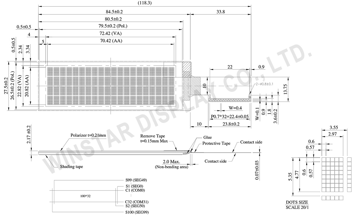
Die Abmessungen des Moduls betragen 84,5 x 27,5 mm bei einer Dicke von 2,17 mm, und die aktive Fläche ist 70,42 x 20,82 mm groß, mit einer Diagonale von 2,89 Zoll. Ausgestattet mit einem SSD1311-Treiber-IC unterstützt der WEO002004C ein integriertes Zeichensatzsystem, einschließlich ASCII, Englisch, Europäisch und Japanisch. Jedes Zeichen besteht aus 5x8 Pixeln, was eine detaillierte und klare Textdarstellung gewährleistet.

Der Anzeigemodus dieses Moduls ist 4 Zeilen, wobei jede Zeile 20 Zeichen darstellen kann. Aufgrund der selbstleuchtenden Eigenschaft der OLED-Technologie benötigt dieses Modul keine Hintergrundbeleuchtung, was zu einem leichteren und dünneren Design führt und das Kontrastverhältnis auf 10.000:1 erhöht. Zudem bietet es einen ultraweiten Betrachtungswinkel von bis zu 175 Grad, der eine konsistente Anzeigequalität aus verschiedenen Blickwinkeln gewährleistet. Das Modul bietet auch einen niedrigen Stromverbrauch und einen breiten Betriebstemperaturbereich, was seine Vielseitigkeit unterstreicht.

Der Betriebstemperaturbereich des WEO002004C reicht von -40°C bis +80°C, der Lagertemperaturbereich von -40°C bis +85°C, was eine stabile Leistung unter extremen Bedingungen ermöglicht. Das Modul arbeitet innerhalb eines logischen Spannungsbereichs von 2,4V bis 3,3V, typischerweise 3V, und verwendet eine 1/32 Duty-Treibermethode.

Darüber hinaus unterstützt der WEO002004C mehrere Schnittstellenoptionen, einschließlich 6800/8080 8-Bit Parallel- und I2C/SPI Seriell-Schnittstellen, die eine flexible Verbindung bieten, um unterschiedlichen Systemanforderungen gerecht zu werden. Die Modulreihe bietet auch verschiedene Optionen für Flexible Printed Circuit (FPC), um unterschiedliche Kundenbedürfnisse zu erfüllen.

Mit seiner zuverlässigen Anzeigequalität, dem breiten Betriebstemperaturbereich und den flexiblen Schnittstellenoptionen ist das WEO002004C OLED-Display-Modul mit SSD1311-Treiber-IC eine praktische Alternative zu herkömmlichen LCD-Modulen. Wir empfehlen, dieses 4x20-Zeichen-OLED-Modul in Betracht zu ziehen, um die Anzeigeleistung Ihres Produkts zu verbessern und eine überlegene Anzeigequalität bei geringerem Energieverbrauch zu erzielen.


   FPC-Optionen


Zeichnung

SSD1331 OLED Display, 2.89 inches 20x4 COG OLED SSD1311 - WEO002004C

Data source ref: WEO002004CLPP5N00000

Technische Daten

Schnittstelle Pin-Funktion

Pin No. Symbol Pin Type Beschreibung
1 NC No connection
2 VSL P This is segment voltage (output low level) reference pin.  
When external VSL is not used, this pin should be left open. 
When external VSL is used, connect with resistor and diode to ground (details depend on application).
3 VSS P Ground pin.  It must be connected to external ground.  
4 REGVDD I Internal VDD regulator selection pin in 5V I/O application mode.  
When this pin is pulled HIGH, internal VDD regulator is enabled (5V I/O application). 
When this pin is pulled LOW, internal VDD regulator is disabled (Low voltage I/O application).  
5 SHLC I This pin is used to determine the Common output scanning direction.
COM scan direction
SHLC COM scan direction
1 COM0 to COM31   (Normal)
0 COM31 to COM0   (Reverse)
Note
(1) 0 is connected to VSS
(2) 1 is connected to VDDIO
6 SHLS I This pin is used to change the mapping between the display data column address and the Segment driver. 
SEG scan direction
SHLS SEG direction
1 SEG0 to SEG99  (Normal)
0 SEG99 to SEG0  (Reverse)
Note
(1) 0 is connected to VSS
(2) 1 is connected to VDDIO
7 VDD P Power supply for core logic operation.  
VDD can be supplied externally or regulated internally.   
In LV IO application (internal VDD is disabled), this is a power input pin.
In 5V IO application (internal VDD is enabled), VDD is regulated internally from VDDIO. 
A capacitor should be connected between VDD and VSS under all circumstances.
8 VDDIO P Low voltage power supply and power supply for interface logic level in both Low Voltage I/O and 5V I/O application.  It should match with the MCU interface voltage level and must be connected to external source.
9 BS0 I MCU bus interface selection pins.  Select appropriate logic setting as described in the following table. BS2, BS1 and BS0 are pin select.
Bus Interface selection
BS[2:0] Interface
000 Serial Interface
001 Invalid
010 I2C
011 Invalid
100 8-bit 6800 parallel
101 4-bit 6800 parallel
110 8-bit 8080 parallel
111 4-bit 8080 parallel
Note
(1) 0 is connected to VSS
(2) 1 is connected to VDDIO
10 BS1
11 BS2
12 GPIO I/O It is a GPIO pin. Details refer to OLED command DCh.
13 CS# I This pin is the chip select input connecting to the MCU.  
The chip is enabled for MCU communication only when CS# is pulled LOW (active LOW).
In I2C mode, this pin must be connected to VSS.  
14 RES# I This pin is reset signal input.  
When the pin is pulled LOW, initialization of the chip is executed.
Keep this pin pull HIGH during normal operation.
15 D/C# I This pin is Data/Command control pin connecting to the MCU.
When the pin is pulled HIGH, the data at D[7:0] will be interpreted as data. 
When the pin is pulled LOW, the data at D[7:0] will be transferred to a command register.   
In I2C mode, this pin acts as SA0 for slave address selection.
When serial interface is selected, this pin must be connected to VSS.
16 R/W#(WR#) I This pin is read / write control input pin connecting to the MCU interface.  
When 6800 interface mode is selected, this pin will be used as Read/Write (R/W#) selection input. Read mode will be carried out when this pin is pulled HIGH and write mode when LOW. 
When 8080 interface mode is selected, this pin will be the Write (WR#) input. Data write operation is initiated when this pin is pulled LOW and the chip is selected.
When serial or I2C interface is selected, this pin must be connected to VSS.
17 E(RD#) I This pin is MCU interface input.  
When 6800 interface mode is selected, this pin will be used as the Enable (E) signal.
Read/write operation is initiated when this pin is pulled HIGH and the chip is selected.
When 8080 interface mode is selected, this pin receives the Read (RD#) signal. Read operation is initiated when this pin is pulled LOW and the chip is selected.  
When serial or I2C interface is selected, this pin must be connected to VSS.
18 D0 I/O These pins are bi-directional data bus connecting to the MCU data bus. 
Unused pins are recommended to tie LOW.   
When serial interface mode is selected, D0 will be the serial clock input: SCLK; D1 will be the serial data input: SID and D2 will be the serial data output: SOD.
When I2C mode is selected, D2, D1 should be tied together and serve as SDAout, SDAin in application and D0 is the serial clock input, SCL.
19 D1
20 D2
21 D3
22 D4
23 D5
24 D6
25 D7
26 IREF I This pin is the segment output current reference pin.  
IREF is supplied externally.  
A resistor should be connected between this pin and VSS to maintain current of around 15uA.
27 ROM0 I These pins are used to select Character ROM; select appropriate logic setting as described in the following table.  ROM1 and ROM0 are pin select as shown in below table:
Character ROM selection
ROM1 ROM0 ROM
0 0 A
0 1 B
1 0 C
1 1 S/W selectable(3)
Note
(1) 0 is connected to VSS
(2) 1 is connected to VDDIO
28 ROM1
29 OPR0 I This pin is used to select the character number of character generator. 
Character RAM selection
OPR1 OPR0 CGROM CGRAM
1 1 256 0
0 1 248 8
1 0 250 6
0 0 240 8

Note
(1) 0 is connected to VSS
(2) 1 is connected to VDDIO
30 OPR1
31 VCOMH P COM signal deselected voltage level.  
A capacitor should be connected between this pin and VSS.  
No external power supply is allowed to connect to this pin. 
32 VCC P Power supply for panel driving voltage.  This is also the most positive power voltage supply pin. It is supplied by external high voltage source.
33 NC No connection

mechanische Daten

Artikel Ausmaß Einheit
Anzeigeformat 20 Zeichen × 4 Zeilen
Abmaße der modul 84,5 x 27,5 x 2,17 mm
Anzeigebereich 72,42 x 22,82 mm
Aktiver Bereich 70,42 x 20,82 mm
Punktgröße 0,57 x 0,57 mm
Punktabstand 0,60 x 0,60 mm
Zeichengröße 2,97 x 4,77 mm
Character pitch 3,55 x 5,35 mm
LCD-Typ OLED , Monochrome
Duty 1/32
IC SSD1311
Schnittstelle 6800,8080,SPI,I2C
Größe (Diagonale) 2,89 Zoll

Absolute Grenzwerte

Artikel Symbol Mindestwert Maximalwert Einheit
Supply Voltage For Logic VDD -0,3 VDDIO V
Power Supply for I/O pins VDDIO -0,3 6 V
Operating Voltage VCC 0 16 V
Betriebstemperatur TOP -40 +80 °C
Lagertemperatur TST -40 +85 °C
 

elektronische Eingenschaften

DC elektronische Eingenschaften

Artikel Symbol Bedingung Mindestwert typischer Wert Maximalwert Einheit
Supply Voltage For Logic VDD Low Voltage I/O 2,4 3,0 3,3 V
5V I/O
(VDD as output)
V
Power supply for I/O pins VDDIO Low Voltage I/O 2,4 3,0 3,3 V
5V I/O 4,4 5,0 5,3 V
Operating Voltage VCC 8,0 10,0 10,5 V
8,0 12,0 12,5 V
Input High Volt. VIH 0,8xVDDIO V
Input Low Volt. VIL 0,2xVDDIO V
Output High Volt. VOH IOH=-0,5mA 0,9xVDDIO V
Output Low Volt. VOL IOL=0,5mA 0,1xVDDIO V
50% Check Board Operating Current ICC VCC=10V 19 29 mA
VCC=12V 23 35 mA

FPC-Optionen:

Bild FPC Length PIN pitch ZIF FPC or HOTBAR FPC Schnittstelle FPC No. Create Date
FPC2070003111XXXXX00_WEO002004CLPP5N00000 35,2 31 0,7 BOTBAR FPC 6800,8080,SPI,I2C FPC2070003111XXXXX00 20120921
FPC2005003421XXXXX00_WEO002004CLPP5N00001 31 34 0,5 ZIF FPC 6800,8080,SPI,I2C FPC2005003421XXXXX00 20151223

Ähnliche Produkte

go top
close

Wir schätzen Ihre Privatsphäre

Durch Klicken auf „Alle Cookies zulassen“ stimmen Sie der Speicherung von Cookies auf Ihrem Gerät zu, um die Navigation auf der Website zu verbessern, die Nutzung der Website zu analysieren und unsere Marketing- und Leistungsbemühungen zu unterstützen. Weitere Informationen zu diesem Thema finden Sie in unserer Richtlinie. Datenschutzrichtlinie

Wir schätzen Ihre Privatsphäre

Winstar und bestimmte Drittparteien verwenden Cookies auf www.winstar.com.tw. Die Einzelheiten zu den Arten von Cookies, ihrem Zweck und den beteiligten Drittparteien sind unten sowie in unserer Cookie-Richtlinie beschrieben. Klicken Sie auf „Alle zulassen“, um unserer Verwendung von Cookies zuzustimmen und die bestmögliche Erfahrung auf unseren Websites zu erzielen. Sie können auch Ihre Präferenzen festlegen oder Cookies ablehnen (mit Ausnahme der unbedingt erforderlichen Cookies).

Einwilligungspräferenzen verwalten

Immer aktiv
Notwendige Cookies

Diese Cookies sind unerlässlich, um Ihnen das Navigieren auf der Website zu ermöglichen und ihre Funktionen zu nutzen, wie z. B. das Festlegen Ihrer Datenschutzpräferenzen, das Einloggen oder das Ausfüllen von Formularen.

Analyse-Cookies

Diese Cookies, auch als „Statistik-Cookies“ bekannt, sammeln Informationen darüber, wie Sie eine Website nutzen, z. B. welche Seiten Sie besucht und auf welche Links Sie geklickt haben. Siehe Details.