Home Produtos Display OLED Display OLED Caractere WEO002004C

Módulo de Display OLED 20x4 COG SSD1311 2,89"

Model No. WEO002004C

►Tipo: Caractere
►Estrutura: COG
►20 caracteres x 4 linhas
►IC:SSD1311
►Alimentação 3V/5V
►1/32 duty
►Interface: 6800, 8080, SPI, I2C
►Display Color: Branco / Amarelo
►Other FPC options available in below table

Descrição

O módulo de display OLED 20x4 COG SSD1311 (Modelo: WEO002004C) apresenta um design COG (Chip On Glass), oferecendo uma solução de display de alta performance e confiabilidade. Este módulo de display OLED SSD1311 é conhecido pela sua excelente qualidade de exibição e durabilidade, tornando-o ideal para uma variedade de aplicações.

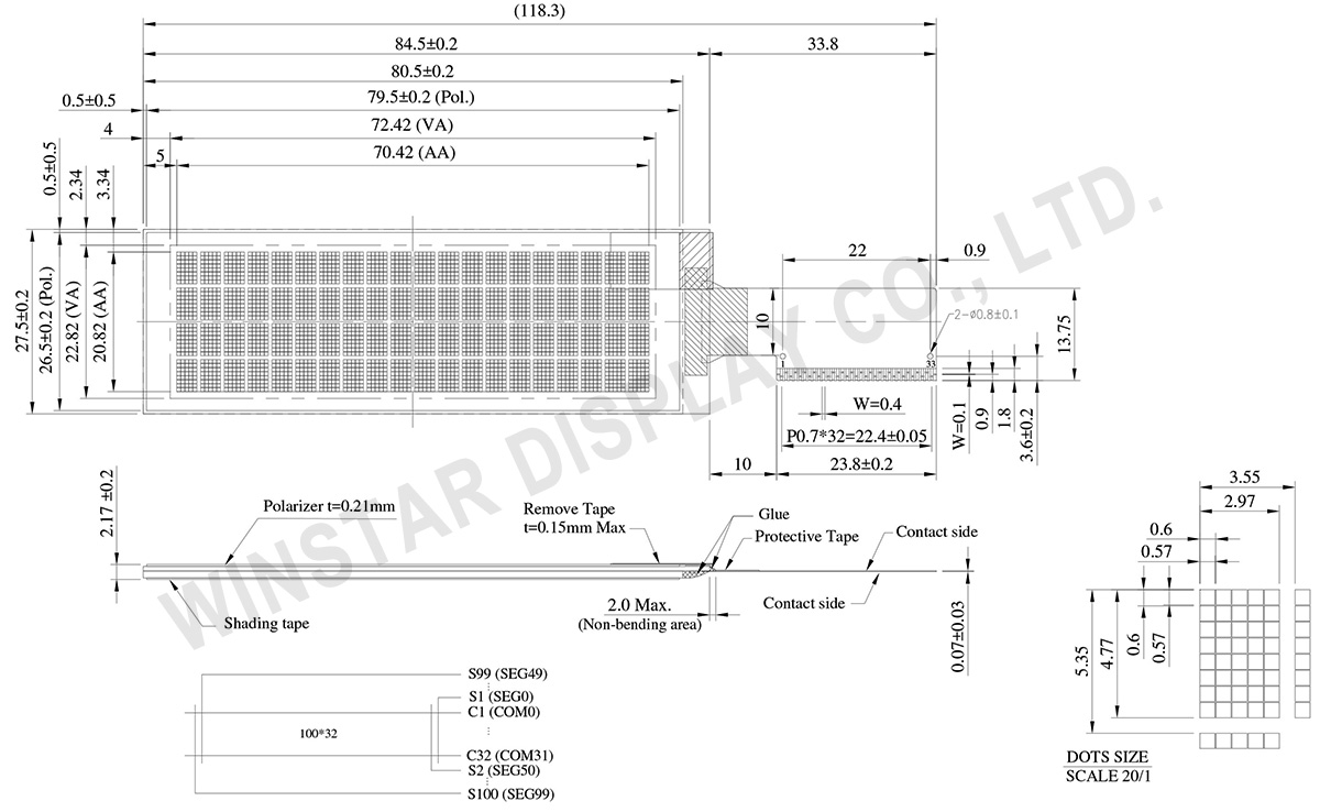
As dimensões do módulo são 84,5 x 27,5 mm com uma espessura de 2,17 mm, e a área ativa é de 70,42 x 20,82 mm, com um tamanho diagonal de 2,89 polegadas. Equipado com um IC controlador SSD1311, o WEO002004C suporta um conjunto de caracteres integrado, incluindo caracteres ASCII, ingleses, europeus e japoneses. Cada caractere é composto por 5x8 pixels, garantindo uma representação detalhada e clara do texto.

O modo de exibição deste módulo é de 4 linhas, com cada linha capaz de mostrar 20 caracteres. Devido à natureza auto-emissiva da tecnologia OLED, este módulo não requer retroiluminação, resultando em um design mais leve e fino, além de uma relação de contraste aprimorada de 10.000:1. Além disso, oferece um ângulo de visão ultra-amplo de até 175 graus, garantindo uma qualidade de exibição consistente a partir de vários ângulos. O módulo também apresenta baixo consumo de energia e uma ampla faixa de temperatura de operação, demonstrando sua versatilidade.

A faixa de temperatura de operação do WEO002004C é de -40°C a +80°C, com uma faixa de temperatura de armazenamento de -40°C a +85°C, permitindo um desempenho estável em condições extremas. O módulo opera dentro de uma faixa de tensão lógica de 2,4V a 3,3V, com um valor típico de 3V, e utiliza um método de acionamento de 1/32 duty.

Além disso, o WEO002004C suporta várias opções de interface, incluindo interfaces paralelas de 8 bits 6800/8080 e interfaces seriais I2C/SPI, oferecendo conectividade flexível para atender diferentes requisitos de sistema. A série de módulos também oferece várias opções de Circuito Impresso Flexível (FPC) para atender às diversas necessidades dos clientes.

Com sua qualidade de exibição confiável, ampla faixa de temperatura de operação e opções flexíveis de interface, o módulo OLED WEO002004C com IC controlador SSD1311 é uma alternativa prática aos módulos LCD tradicionais. Recomendamos considerar este módulo OLED 20x4 para melhorar o desempenho de exibição do seu produto, alcançando uma qualidade superior de exibição e menor consumo de energia.


   FPC Options


DRAWING

SSD1331 OLED Display, 2.89 inches 20x4 COG OLED SSD1311 - WEO002004C

Data source ref: WEO002004CLPP5N00000

SPECIFICATIONS

Função do pino de interface

Pin No. Símbolo Pin Type Descrição
1 NC No connection
2 VSL P This is segment voltage (output low level) reference pin.  
When external VSL is not used, this pin should be left open. 
When external VSL is used, connect with resistor and diode to ground (details depend on application).
3 VSS P Ground pin.  It must be connected to external ground.  
4 REGVDD I Internal VDD regulator selection pin in 5V I/O application mode.  
When this pin is pulled HIGH, internal VDD regulator is enabled (5V I/O application). 
When this pin is pulled LOW, internal VDD regulator is disabled (Low voltage I/O application).  
5 SHLC I This pin is used to determine the Common output scanning direction.
COM scan direction
SHLC COM scan direction
1 COM0 to COM31   (Normal)
0 COM31 to COM0   (Reverse)
Note
(1) 0 is connected to VSS
(2) 1 is connected to VDDIO
6 SHLS I This pin is used to change the mapping between the display data column address and the Segment driver. 
SEG scan direction
SHLS SEG direction
1 SEG0 to SEG99  (Normal)
0 SEG99 to SEG0  (Reverse)
Note
(1) 0 is connected to VSS
(2) 1 is connected to VDDIO
7 VDD P Power supply for core logic operation.  
VDD can be supplied externally or regulated internally.   
In LV IO application (internal VDD is disabled), this is a power input pin.
In 5V IO application (internal VDD is enabled), VDD is regulated internally from VDDIO. 
A capacitor should be connected between VDD and VSS under all circumstances.
8 VDDIO P Low voltage power supply and power supply for interface logic level in both Low Voltage I/O and 5V I/O application.  It should match with the MCU interface voltage level and must be connected to external source.
9 BS0 I MCU bus interface selection pins.  Select appropriate logic setting as described in the following table. BS2, BS1 and BS0 are pin select.
Bus Interface selection
BS[2:0] Interface
000 Serial Interface
001 Invalid
010 I2C
011 Invalid
100 8-bit 6800 parallel
101 4-bit 6800 parallel
110 8-bit 8080 parallel
111 4-bit 8080 parallel
Note
(1) 0 is connected to VSS
(2) 1 is connected to VDDIO
10 BS1
11 BS2
12 GPIO I/O It is a GPIO pin. Details refer to OLED command DCh.
13 CS# I This pin is the chip select input connecting to the MCU.  
The chip is enabled for MCU communication only when CS# is pulled LOW (active LOW).
In I2C mode, this pin must be connected to VSS.  
14 RES# I This pin is reset signal input.  
When the pin is pulled LOW, initialization of the chip is executed.
Keep this pin pull HIGH during normal operation.
15 D/C# I This pin is Data/Command control pin connecting to the MCU.
When the pin is pulled HIGH, the data at D[7:0] will be interpreted as data. 
When the pin is pulled LOW, the data at D[7:0] will be transferred to a command register.   
In I2C mode, this pin acts as SA0 for slave address selection.
When serial interface is selected, this pin must be connected to VSS.
16 R/W#(WR#) I This pin is read / write control input pin connecting to the MCU interface.  
When 6800 interface mode is selected, this pin will be used as Read/Write (R/W#) selection input. Read mode will be carried out when this pin is pulled HIGH and write mode when LOW. 
When 8080 interface mode is selected, this pin will be the Write (WR#) input. Data write operation is initiated when this pin is pulled LOW and the chip is selected.
When serial or I2C interface is selected, this pin must be connected to VSS.
17 E(RD#) I This pin is MCU interface input.  
When 6800 interface mode is selected, this pin will be used as the Enable (E) signal.
Read/write operation is initiated when this pin is pulled HIGH and the chip is selected.
When 8080 interface mode is selected, this pin receives the Read (RD#) signal. Read operation is initiated when this pin is pulled LOW and the chip is selected.  
When serial or I2C interface is selected, this pin must be connected to VSS.
18 D0 I/O These pins are bi-directional data bus connecting to the MCU data bus. 
Unused pins are recommended to tie LOW.   
When serial interface mode is selected, D0 will be the serial clock input: SCLK; D1 will be the serial data input: SID and D2 will be the serial data output: SOD.
When I2C mode is selected, D2, D1 should be tied together and serve as SDAout, SDAin in application and D0 is the serial clock input, SCL.
19 D1
20 D2
21 D3
22 D4
23 D5
24 D6
25 D7
26 IREF I This pin is the segment output current reference pin.  
IREF is supplied externally.  
A resistor should be connected between this pin and VSS to maintain current of around 15uA.
27 ROM0 I These pins are used to select Character ROM; select appropriate logic setting as described in the following table.  ROM1 and ROM0 are pin select as shown in below table:
Character ROM selection
ROM1 ROM0 ROM
0 0 A
0 1 B
1 0 C
1 1 S/W selectable(3)
Note
(1) 0 is connected to VSS
(2) 1 is connected to VDDIO
28 ROM1
29 OPR0 I This pin is used to select the character number of character generator. 
Character RAM selection
OPR1 OPR0 CGROM CGRAM
1 1 256 0
0 1 248 8
1 0 250 6
0 0 240 8

Note
(1) 0 is connected to VSS
(2) 1 is connected to VDDIO
30 OPR1
31 VCOMH P COM signal deselected voltage level.  
A capacitor should be connected between this pin and VSS.  
No external power supply is allowed to connect to this pin. 
32 VCC P Power supply for panel driving voltage.  This is also the most positive power voltage supply pin. It is supplied by external high voltage source.
33 NC No connection

Dados Mecânicos

Item Dimensão Unidade
Number of Characters 20 Caracteres x 4 Linhas
Dimensão do módulo 84.5 x 27.5 x 2.17 mm
Área de visualização 72.42 x 22.82 mm
Área ativa 70.42 x 20.82 mm
Tamanho do ponto 0.57 x 0.57 mm
Distância entre pontos 0.60 x 0.60 mm
Tamanho do Caracteres 2.97 x 4.77 mm
Distância entre Caracteres 3.55 x 5.35 mm
LCD type OLED , Monochrome
Duty 1/32
IC SSD1311
Interface 6800,8080,SPI,I2C
Tamanho 2,89 polegadas

Classificações Máximas Absolutas

Item Símbolo Valor Min Valor Máximo Unidade
Supply Voltage For Logic VDD -0.3 VDDIO V
Power Supply for I/O pins VDDIO -0.3 6 V
Operating Voltage VCC 0 16 V
Temperatura de operação TOP -40 +80 °C
Temperatura de armazenamento TST -40 +85 °C
 

Características Eletrônicas

DC Características Eletrônicas

Item Símbolo Condição Valor Min Valor Típico Valor Máximo Unidade
Supply Voltage For Logic VDD Low Voltage I/O 2.4 3.0 3.3 V
5V I/O
(VDD as output)
V
Power supply for I/O pins VDDIO Low Voltage I/O 2.4 3.0 3.3 V
5V I/O 4.4 5.0 5.3 V
Operating Voltage VCC 8.0 10.0 10.5 V
8.0 12.0 12.5 V
Input High Volt. VIH 0.8xVDDIO V
Input Low Volt. VIL 0.2xVDDIO V
Output High Volt. VOH IOH=-0.5mA 0.9xVDDIO V
Output Low Volt. VOL IOL=0.5mA 0.1xVDDIO V
50% Check Board Operating Current ICC VCC=10V 19 29 mA
VCC=12V 23 35 mA

FPC Options:

Drawing FPC Length PIN pitch ZIF FPC or HOTBAR FPC Interface FPC No. Create Date
FPC2070003111XXXXX00_WEO002004CLPP5N00000 35.2 31 0.7 BOTBAR FPC 6800,8080,SPI,I2C FPC2070003111XXXXX00 20120921
FPC2005003421XXXXX00_WEO002004CLPP5N00001 31 34 0.5 ZIF FPC 6800,8080,SPI,I2C FPC2005003421XXXXX00 20151223

Related Products

go top
close

Valorizamos sua privacidade

Ao clicar em "Permitir todos os cookies", você concorda com o armazenamento de cookies no seu dispositivo para melhorar a navegação no site, analisar o uso do site e auxiliar nossos esforços de marketing e desempenho. Você pode encontrar mais informações sobre esse assunto em nossa política. Política de privacidade

Valorizamos sua privacidade

A Winstar e certos terceiros utilizam cookies no site www.winstar.com.tw. Os detalhes sobre os tipos de cookies, sua finalidade e as partes terceiras envolvidas estão descritos abaixo e em nossa Política de Cookies. Clique em “Permitir todos” para consentir o uso de cookies e obter a melhor experiência possível em nossos sites. Você também pode definir suas preferências ou rejeitar cookies (exceto os estritamente necessários).

Gerenciar preferências de consentimento

Sempre ativo
Cookies essenciais

Esses cookies são essenciais para permitir que você navegue pelo site e utilize seus recursos, como definir suas preferências de privacidade, fazer login ou preencher formulários.

Cookies de análise

Também conhecidos como "cookies estatísticos", esses cookies coletam informações sobre como você utiliza um site, como quais páginas você visitou e em quais links você clicou. Veja os detalhes.