
 - WO160160A")
私たちはあなたのプライバシーを大切にします
「すべてのクッキーを許可」をクリックすると、サイトのナビゲーションを向上させ、サイト使用状況を分析し、マーケティングおよびパフォーマンスの取り組みを支援するために、クッキーをデバイスに保存することに同意したことになります。この件に関する詳細情報は、ポリシーをご覧ください。プライバシーポリシー


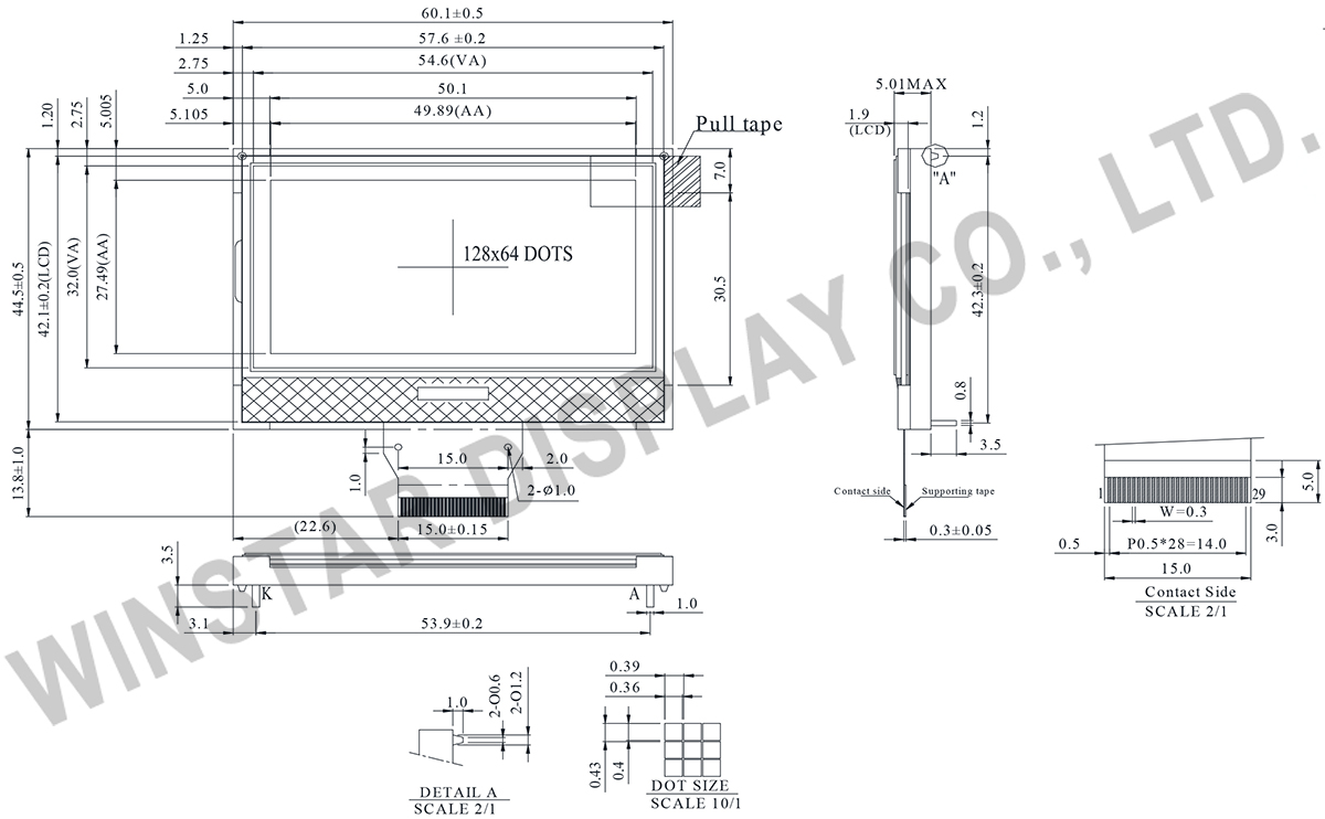
WO12864A1は、2.24インチ 128x64 COGグラフィックLCDモジュールです。ST7565PコントローラICまたは互換ICを搭載し、6800 8-bit、8080 8-bitパラレルインターフェース、および4線式SPIインターフェースに対応しています。
モジュール外形寸法は60.1 × 44.5 mm、表示エリアは54.6 × 32.0 mm、有効表示エリアは49.89 × 27.49 mmです。LEDバックライトを採用し、1/65 Duty、1/9 Biasで駆動します。
動作温度範囲は-20℃~+70℃、保存温度範囲は-30℃~+80℃で、産業機器、ハンディ端末、計測機器、医療機器をはじめ、各種組込み機器に適しています。
| 項目 | 標準値 | 単位 |
|---|---|---|
| 表示ドット数 | 128 x 64 | - |
| モジュールサイズ | 60.1 x 44.5 x 5.01(MAX) | mm |
| 表示エリア | 54.6 x 32.0 | mm |
| 有効エリア | 49.89 x 27.49 | mm |
| ドットサイズ | 0.36 x 0.4 | mm |
| ドットピッチ | 0.39 x 0.43 | mm |
| 駆動方法 | 1/65 , 1/9 Bias | |
| バックライトタイプ | LED | |
| IC | ST7565P | |
| インターフェイス | 6800/8080/4-Line SPI | |
| 項目 | 記号 | 最小値 | 典型値 | 最大値 | 単位 |
|---|---|---|---|---|---|
| 操作温度 | TOP | -20 | - | +70 | ℃ |
| 保存温度 | TST | -30 | - | +80 | ℃ |
| 電源電圧 | VDD | -0.3 | - | 3.6 | V |
| Power supply voltage (VDD standard) | V0,VOUT | -0.3 | - | 14.5 | V |
| Power supply voltage (VDD standard) | V1,V2,V3,V4 | -0.3 | - | V0+0.3 | V |
| 項目 | 記号 | 条件 | 最小値 | 典型値 | 最大値 | 単位 |
|---|---|---|---|---|---|---|
| ロジック電源電圧 | VDD-VSS | - | 2.7 | 3.0 | 3.3 | V |
| LCM供給電圧 | V0-VSS | Ta=-20℃ Ta=25℃ Ta=70℃ |
- 9.2 - |
- 9.5 - |
- 9.8 - |
V V V |
| 高レベル入力電圧 | VIH | - | 0.8 VDD | - | VDD | V |
| 低レベル入力電圧 | VIL | - | VSS | - | 0.2VDD | V |
| 高レベル出力電圧 | VOH | IOUT=-0.5mA | 0.8VDD | - | VDD | V |
| 低レベル出力電圧 | VOL | IOUT=0.5mA | VSS | - | 0.2VDD | V |
| 供給電流 | IDD | VDD=3.0V | - | 0.1 | 2.0 | mA |
| Pin No. | 記号 | Level | 説明 |
|---|---|---|---|
| 1 | P/S | I | This is the parallel data input/serial data input switch terminal. |
| 2 | C86 | I | This is the MPU interface switch terminal. |
| 3 | VR | I | Output voltage regulator terminal. Provides the voltage between VSS and V0 through a resistive voltage divider. |
| 4~8 | V0~V4 | Power supply | This is a multi-level power supply for the liquid crystal drive. |
| 9 | CAP2N | O | DC/DC voltage converter. Connect a capacitor between this terminal and the CAP2P terminal. |
| 10 | CAP2P | O | DC/DC voltage converter. Connect a capacitor between this terminal and the CAP2N terminal. |
| 11 | CAP1P | O | DC/DC voltage converter. Connect a capacitor between this terminal and the CAP1N terminal. |
| 12 | CAP1N | O | DC/DC voltage converter. Connect a capacitor between this terminal and the CAP1P terminal. |
| 13 | CAP3P | O | DC/DC voltage converter. Connect a capacitor between this terminal and the CAP1N terminal. |
| 14 | VOUT | O | DC/DC voltage converter. Connect a capacitor between this terminal and vss or VDD |
| 15 | VSS | Power supply | Ground |
| 16 | VDD | Power supply | Power supply |
| 17~24 | D7~D0 | I/O | This is an 8-bit bi-directional data bus that connects to an 8-bit or 16-bit standard MPU data bus. |
| 25 | /RD(E) | I | The data bus is in output status when this signal is “L” |
| 26 | /WR(R/W) | I | The data bus are latched at the rising edge of the WR signal |
| 27 | A0 | I | This is connect to the least significant bit of the Norman MPU address bus, and it determines whether the data bits are data or a command. |
| 28 | /RES | I | When RES is set to “L”, the setting are initialized. |
| 29 | /CS1 | I | This is the chip select signal. |

「すべてのクッキーを許可」をクリックすると、サイトのナビゲーションを向上させ、サイト使用状況を分析し、マーケティングおよびパフォーマンスの取り組みを支援するために、クッキーをデバイスに保存することに同意したことになります。この件に関する詳細情報は、ポリシーをご覧ください。プライバシーポリシー