

2.8 inch IPS 240x320 Touch Panel TFT LCD Display
Model No. WF28JTYAJDNF0
►Size: 2.8 inch
►Resolution: 240×320 dots
►View Direction: IPS
►Interface: MCU, SPI
►Driver IC:ILI9341
►Control-Board: No
►Brightness(cd/m²): 400
►Frame Through Hole: No
►Touch Panel: Projected Capacitive Touch Panel (PCAP)
Description
WF28JTYAJDNF0 is a 2.8-inch portrait-mode TFT display module with a resolution of 240x320 pixels, a brightness of 400 cd/m2, and a contrast ratio of 800:1. This LCD module features a projected capacitive touch panel and is equipped with the ILI9341V IC, supporting MCU or SPI interfaces. The module has dimensions of 50.5 x 69.7 mm, with an active area of 43.2 x 57.6 mm. The supply voltage ranges from 1.65V to 3.3V. The projected capacitive touch panel is integrated with the FT6336G IC, supporting the I2C interface and a single detect point. The module can operate within a temperature range of -20°C to +70°C, with storage temperatures ranging from -30°C to +80°C.
WF28JTYAJDNF0 utilizes IPS technology, providing a wide viewing angle of Left: 80 / Right: 80 / Up: 80 / Down: 80 degrees (typical value). IPS panels in TFT displays offer broader viewing angles, accurate and consistent color reproduction, superior image quality, precise touchscreen performance, and consistent color temperature. The versatility of IPS TFT-LCD displays makes them suitable for various applications, including consumer electronics, medical displays, and industrial control panels.
DRAWING
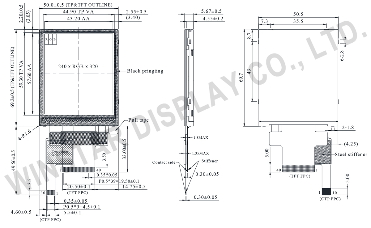
SPECIFICATIONS
Interface Pin Function
LCM PIN Definition
| NO | Symbol | Function | I/O | ||||||||||||||||||||||||||||||||||||||||||||
|---|---|---|---|---|---|---|---|---|---|---|---|---|---|---|---|---|---|---|---|---|---|---|---|---|---|---|---|---|---|---|---|---|---|---|---|---|---|---|---|---|---|---|---|---|---|---|---|
| 1 | GND | Ground | P | ||||||||||||||||||||||||||||||||||||||||||||
| 2-6 | NC | No connection | - | ||||||||||||||||||||||||||||||||||||||||||||
| 7 | VCI | High voltage power supply for analog circuit blocks (2.5 ~ 3.3 V) |
P | ||||||||||||||||||||||||||||||||||||||||||||
| 8 | IOVCC | Low voltage power supply for interface logic circuits (2.5 ~ 3.3 V) |
P | ||||||||||||||||||||||||||||||||||||||||||||
| 9 | TE | Tearing effect output pin to synchronize MPU to frame writing, activated by S/W command. When this pin is not activated, this pin is low. If not used, open this pin. |
O | ||||||||||||||||||||||||||||||||||||||||||||
| 10 | CS | Chip select signal. | I | ||||||||||||||||||||||||||||||||||||||||||||
| 11 | D/CX(SCL) | (D/CX): This pin is used to select "Data or Command" in the parallel interface. When DCX = 1, data is selected. When DCX = 0, command is selected. (SCL): This pin is used as the serial interface clock in 3-wire 9-bit/4-wire 8-bit serial data interface. If not used, this pin should be connected to IOVCC or GND. |
I | ||||||||||||||||||||||||||||||||||||||||||||
| 12 | WR(SPI_D/C) | (WRX) - 8080-Ⅰ/8080-Ⅱ system: Serves as a write signal and writes data at the rising edge. (D/CX) - 4-line system: Serves as the selector of command or parameter. Fix to IOVCC level when not in use. |
I | ||||||||||||||||||||||||||||||||||||||||||||
| 13 | RD | 8080-Ⅰ/8080-Ⅱ system (RDX): Serves as a read signal and MCU read data at the rising edge. Fix to IOVCC level when not in use. |
I | ||||||||||||||||||||||||||||||||||||||||||||
| 14-29 | DB0~DB15 | 18-bit parallel bi-directional data bus for MCU system. Fix to GND level when not in use. |
I/O | ||||||||||||||||||||||||||||||||||||||||||||
| 30 | RESET | (RESX)This signal will reset the device and must be applied to properly initialize the chip. Signal is active low. |
I | ||||||||||||||||||||||||||||||||||||||||||||
| 31 | IM0 | Select the MCU interface mode
MPU Parallel interface bus and serial interface select If use RGB Interface must select serial interface. * : Fix this pin at IOVCC or GND. |
I | ||||||||||||||||||||||||||||||||||||||||||||
| 32 | IM1 | ||||||||||||||||||||||||||||||||||||||||||||||
| 33 | IM2 | ||||||||||||||||||||||||||||||||||||||||||||||
| 34 | DB16 | 18-bit parallel bi-directional data bus for MCU system and RGB interface mode Fix to GND level when not in use. |
I/O | ||||||||||||||||||||||||||||||||||||||||||||
| 35 | DB17 | ||||||||||||||||||||||||||||||||||||||||||||||
| 36 | LEDK | Cathode of LED backlight. | P | ||||||||||||||||||||||||||||||||||||||||||||
| 37 | LEDK | Cathode of LED backlight. | P | ||||||||||||||||||||||||||||||||||||||||||||
| 38 | LEDA | Anode of LED backlight. | P | ||||||||||||||||||||||||||||||||||||||||||||
| 39 | SDA | SDA : Serial in/out signal. The data is applied on the rising edge of the SCL signal. If not used, fix this pin at IOVCC or GND. |
I/O | ||||||||||||||||||||||||||||||||||||||||||||
| 40 | NC | Not used, open this pin | N | ||||||||||||||||||||||||||||||||||||||||||||
PCAP PIN Definition
| Pin | Symbol | Function |
|---|---|---|
| 1 | VSS | Ground for analog circuit |
| 2 | VDDT | Power Supply : +3.3V |
| 3 | SCL | I2C clock input |
| 4 | NC | No connect |
| 5 | SDA | I2C data input and output |
| 6 | NC | No connect |
| 7 | /RST | External Reset, Low is active |
| 8 | NC | No connect |
| 9 | /INT | External interrupt to the host |
| 10 | VSS | Ground for analog circuit |
General Specifications
| Item | Dimension | Unit |
|---|---|---|
| Size | 2.8 | inch |
| Dot Matrix | 240 x RGB x 320(TFT) | dots |
| Module dimension | 50.5(W) x 69.7(H) x5.67(D) | mm |
| Active Area (AA) | 43.2 x 57.6 | mm |
| Dot pitch | 0.18 x 0.18 | mm |
| LCD type | TFT, Normally Black, Transmissive | |
| TFT Driver IC | ILI9341V or Equivalent | |
| TFT Interface | MCU/SPI | |
| Viewing angle | 80/80/80/80 | |
| Aspect Ratio | 3:4 | |
| Backlight Type | LED,Normally White | |
| PCAP IC | FT6336G or Equivalent | |
| PCAP Interface | I2C | |
| PCAP FW | 0x11 | |
| Touch Panel | Projected Capacitive Touch Panel (PCAP) | |
| Surface | Glare | |
Absolute Maximum Ratings
| Item | Symbol | Min | Typ | Max | Unit |
|---|---|---|---|---|---|
| Operating Temperature | TOP | -20 | - | +70 | ℃ |
| Storage Temperature | TST | -30 | - | +80 | ℃ |
Electrical Characteristics
Operating conditions
| Item | Symbol | Condition | Min | Typ | Max | Unit |
|---|---|---|---|---|---|---|
| Supply Voltage for digital | IOVCC | - | 1.65 | - | 3.3 | V |
| Supply Voltage for analog | VCI | - | 2.5 | - | 3.3 | V |
| Supply Voltage For Touch Logic | VDDT | - | 3.0 | 3.3 | 3.6 | V |
| Power Supply for Current | ICC | IOVCC=VCI =VCC=3.0V |
- | 13 | 20 | mA |
LED driving conditions
| Parameter | Symbol | Min | Typ | Max | Unit |
|---|---|---|---|---|---|
| LED current | - | - | 80 | - | mA |
| LED voltage | LEDA | 8.1 | 9.3 | 10.5 | V |
| LED Life Time | - | 50000 | - | - | Hr |
