


Écran 2.8 pouces IPS TFT LCD Écran Tactile avec 240x320 Résolution
N° de modèle WF28JTYAJDNF0
►Dimension: 2.8 pouces
►Résolution d’écran: 240 x 320 points
►Vue préférentielle 6h
►Interface: MCU, SPI
►CI pilote:ILI9341
►Carte de contrôle : NON
►Luminosité (Cd/m²): 400
►Holding frame with fixing points: NON
►Dalle tactile: avec dalle tactile capacitive (PCAP)
Description
WF28JTYAJDNF0 est un module d'affichage TFT en mode portrait de 2,8 pouces avec une résolution de 240x320 pixels, une luminosité de 400 cd/m2 et un rapport de contraste de 800:1. Ce module LCD est équipé d'un écran tactile capacitif projeté et de l'IC ILI9341V, prenant en charge les interfaces MCU ou SPI. Le module a des dimensions de 50,5 x 69,7 mm, avec une zone active de 43,2 x 57,6 mm. La tension d'alimentation varie de 1,65V à 3,3V. Le panneau tactile capacitif projeté est intégré à l'IC FT6336G, prenant en charge l'interface I2C et un seul point de détection. Le module peut fonctionner dans une plage de température de -20°C à +70°C, avec des températures de stockage variant de -30°C à +80°C.
WF28JTYAJDNF0 utilise la technologie IPS, offrant un large angle de vision de Gauche : 80 / Droite : 80 / Haut : 80 / Bas : 80 degrés (valeur typique). Les panneaux IPS dans les écrans TFT offrent des angles de vision plus larges, une reproduction précise et cohérente des couleurs, une qualité d'image supérieure, des performances précises du touchscreen, et une température de couleur constante. La polyvalence des écrans TFT-LCD IPS les rend adaptés à diverses applications, y compris l'électronique grand public, les écrans médicaux et les panneaux de contrôle industriels.
DESSIN
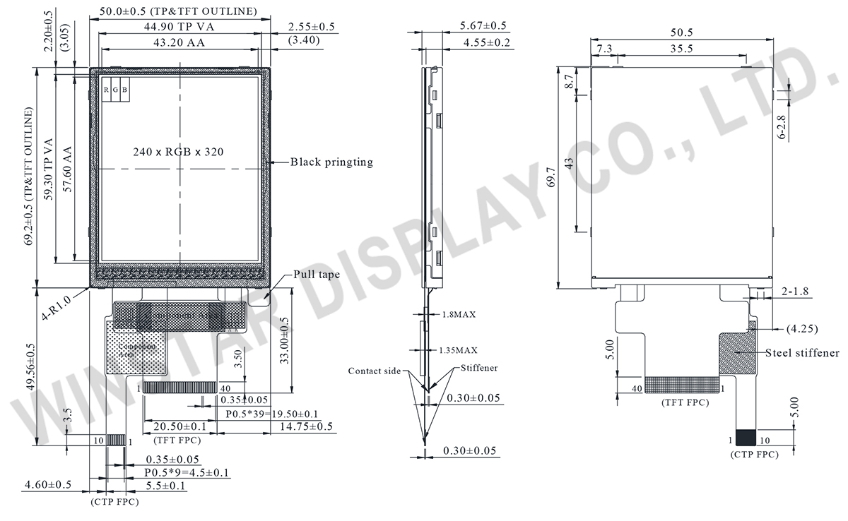
SPÉCIFICATIONS
Fonction PIN sur l'interface
LCM PIN Definition
| NO | Symbole | Fonction | I/O | ||||||||||||||||||||||||||||||||||||||||||||
|---|---|---|---|---|---|---|---|---|---|---|---|---|---|---|---|---|---|---|---|---|---|---|---|---|---|---|---|---|---|---|---|---|---|---|---|---|---|---|---|---|---|---|---|---|---|---|---|
| 1 | GND | Ground | P | ||||||||||||||||||||||||||||||||||||||||||||
| 2-6 | NC | No connection | - | ||||||||||||||||||||||||||||||||||||||||||||
| 7 | VCI | High voltage power supply for analog circuit blocks (2.5 ~ 3.3 V) |
P | ||||||||||||||||||||||||||||||||||||||||||||
| 8 | IOVCC | Low voltage power supply for interface logic circuits (2.5 ~ 3.3 V) |
P | ||||||||||||||||||||||||||||||||||||||||||||
| 9 | TE | Tearing effect output pin to synchronize MPU to frame writing, activated by S/W command. When this pin is not activated, this pin is low. If not used, open this pin. |
O | ||||||||||||||||||||||||||||||||||||||||||||
| 10 | CS | Chip select signal. | I | ||||||||||||||||||||||||||||||||||||||||||||
| 11 | D/CX(SCL) | (D/CX): This pin is used to select "Data or Command" in the parallel interface. When DCX = 1, data is selected. When DCX = 0, command is selected. (SCL): This pin is used as the serial interface clock in 3-wire 9-bit/4-wire 8-bit serial data interface. If not used, this pin should be connected to IOVCC or GND. |
I | ||||||||||||||||||||||||||||||||||||||||||||
| 12 | WR(SPI_D/C) | (WRX) - 8080-Ⅰ/8080-Ⅱ system: Serves as a write signal and writes data at the rising edge. (D/CX) - 4-line system: Serves as the selector of command or parameter. Fix to IOVCC level when not in use. |
I | ||||||||||||||||||||||||||||||||||||||||||||
| 13 | RD | 8080-Ⅰ/8080-Ⅱ system (RDX): Serves as a read signal and MCU read data at the rising edge. Fix to IOVCC level when not in use. |
I | ||||||||||||||||||||||||||||||||||||||||||||
| 14-29 | DB0~DB15 | 18-bit parallel bi-directional data bus for MCU system. Fix to GND level when not in use. |
I/O | ||||||||||||||||||||||||||||||||||||||||||||
| 30 | RESET | (RESX)This signal will reset the device and must be applied to properly initialize the chip. Signal is active low. |
I | ||||||||||||||||||||||||||||||||||||||||||||
| 31 | IM0 | Select the MCU interface mode
MPU Parallel interface bus and serial interface select If use RGB Interface must select serial interface. * : Fix this pin at IOVCC or GND. |
I | ||||||||||||||||||||||||||||||||||||||||||||
| 32 | IM1 | ||||||||||||||||||||||||||||||||||||||||||||||
| 33 | IM2 | ||||||||||||||||||||||||||||||||||||||||||||||
| 34 | DB16 | 18-bit parallel bi-directional data bus for MCU system and RGB interface mode Fix to GND level when not in use. |
I/O | ||||||||||||||||||||||||||||||||||||||||||||
| 35 | DB17 | ||||||||||||||||||||||||||||||||||||||||||||||
| 36 | LEDK | Cathode of LED backlight. | P | ||||||||||||||||||||||||||||||||||||||||||||
| 37 | LEDK | Cathode of LED backlight. | P | ||||||||||||||||||||||||||||||||||||||||||||
| 38 | LEDA | Anode of LED backlight. | P | ||||||||||||||||||||||||||||||||||||||||||||
| 39 | SDA | SDA : Serial in/out signal. The data is applied on the rising edge of the SCL signal. If not used, fix this pin at IOVCC or GND. |
I/O | ||||||||||||||||||||||||||||||||||||||||||||
| 40 | NC | Not used, open this pin | N | ||||||||||||||||||||||||||||||||||||||||||||
PCAP PIN Definition
| Pin | Symbole | Fonction |
|---|---|---|
| 1 | VSS | Ground for analog circuit |
| 2 | VDDT | Power Supply : +3.3V |
| 3 | SCL | I2C clock input |
| 4 | NC | No connect |
| 5 | SDA | I2C data input and output |
| 6 | NC | No connect |
| 7 | /RST | External Reset, Low is active |
| 8 | NC | No connect |
| 9 | /INT | External interrupt to the host |
| 10 | VSS | Ground for analog circuit |
Spécifications générales
| Article | Dimensions | Unité |
|---|---|---|
| Diagonale | 2.8 | pouces |
| Matrice de points (Résolution) | 240 x RGB x 320(TFT) | points |
| Dimensions du module | 50.5(W) x 69.7(H) x5.67(D) | mm |
| Zone active (AA) | 43.2 x 57.6 | mm |
| Pas des points | 0.18 x 0.18 | mm |
| Type de LCD | TFT, Noir, Transmissif | |
| TFT CI pilote | ILI9341V ou équivalent | |
| TFT Interface | MCU/SPI | |
| Vue préférentielle | 80/80/80/80 | |
| Rapport d'aspect | 3:4 | |
| Type de rétroéclairage | LED, Blanc | |
| PCAP IC | FT6336G ou équivalent | |
| PCAP Interface | I2C | |
| PCAP FW | 0x11 | |
| Dalle tactile | Avec dalle tactile capacitive | |
| Surface | Reflets | |
Valeurs nominales maximales absolues
| Article | Symbole | Valeur min | Valeur type | Valeur max | Unité |
|---|---|---|---|---|---|
| Température de fonctionnement | TOP | -20 | - | +70 | ℃ |
| Température de stockage | TST | -30 | - | +80 | ℃ |
Electrical Characteristics
Operating conditions
| Article | Symbole | Condition | Valeur min | Valeur type | Valeur max | Unité |
|---|---|---|---|---|---|---|
| Supply Voltage for digital | IOVCC | - | 1.65 | - | 3.3 | V |
| Supply Voltage for analog | VCI | - | 2.5 | - | 3.3 | V |
| Supply Voltage For Touch Logic | VDDT | - | 3.0 | 3.3 | 3.6 | V |
| Power Supply for Current | ICC | IOVCC=VCI =VCC=3.0V |
- | 13 | 20 | mA |
LED driving conditions
| Parameter | Symbole | Valeur min | Valeur type | Valeur max | Unité |
|---|---|---|---|---|---|
| LED current | - | - | 80 | - | mA |
| LED voltage | LEDA | 8.1 | 9.3 | 10.5 | V |
| LED Life Time | - | 50000 | - | - | Hr |
