


我們重視您的隱私
通過點擊「允許所有 Cookie」,代表您同意在您的設備上存儲 Cookie 以增強網站瀏覽體驗、分析網站使用情況並協助我們的行銷和網站效能優化工作。您可以在我們的隱私權政策中找到有關於此的更多資訊。


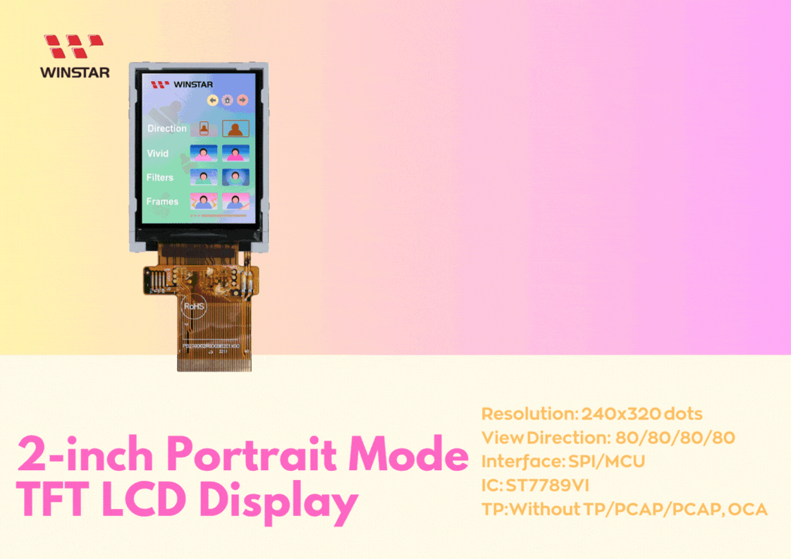
WF0200BTYAJDNG10是一款2吋電容式觸控 IPS TFT LCD 顯示器模組,解析度為240x320像素。模組內建ST7789VI驅動IC,支援MCU 和SPI介面傳輸,觸控面板內建 GT911 IC 可支援I2C介面。WF0200B系列另有無觸控面板模組,此外,PCAP 面板採用 OCA 技術以提高其耐用性並呈現更好的光學清晰度。
此款模組採用IPS面板,具有更寬廣視角的優勢,視角左:80/右:80/上:80/下:80度(典型值),對比度 800:1(典型值),亮度400 nits(典型值),長寬比3:4,供電電壓為2.4V~3.6V,典型值為3.3V。此模組可在-20℃~+70℃溫度範圍下作業;儲存溫度範圍-30℃~+80℃。
2吋直立式TFT液晶顯示螢幕適用於多種電子設備,包括雷射測距儀、空氣品質偵測儀等測量工具,以及偵測設備、運動手錶和其他電子設備。我們的 WF0200B TFT 系列提供無觸摸面板選項; 請查看 WF0200BSYAJDNN0 的網頁了解更多訊息。
| 項目 | 規格 | 單位 |
|---|---|---|
| 顯示尺寸(對角線) | 2 | 吋 |
| 點陣(解析度) | 240 x RGB x 320(TFT) | dots |
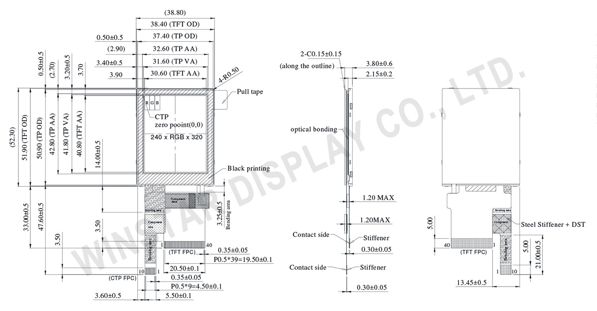
| 模組尺寸 | 38.8(W) x 52.3(H) x3.8(D) | mm |
| 有效區域 | 30.60 x 40.80 | mm |
| 像素間距 | 0.1275 x 0.1275 | mm |
| LCD 類型 | TFT全透 | |
| TFT介面 | MCU / SPI | |
| TFT驅動 IC | ST7789VI 或相容IC | |
| 視角 | 80/80/80/80 (IPS) | |
| 長寬比 | 3:4 | |
| 背光類型 | LED, 白色 | |
| PCAP驅動IC | GT911或相容IC | |
| PCAP介面 | I2C | |
| FW版本 | V92 | |
| PCAP解析度 | 240 * 320 | |
| 觸控面板類型 | PCAP電容式觸控面板 | |
| 表面 | 亮面 | |
| 項目 | 符號 | 最小值 | 典型值 | 最大值 | 單位 |
|---|---|---|---|---|---|
| 工作溫度 | TOP | -20 | - | 70 | ℃ |
| 儲存溫度 | TST | -30 | - | 80 | ℃ |
| 項目 | 符號 | 條件 | 最小值 | 典型值 | 最大值 | 單位 |
|---|---|---|---|---|---|---|
| 類比電源電壓 | VDD | - | 2.4 | 3.3 | 3.6 | V |
| 介面工作電壓 | VDDI | - | 1.65 | 1.8 | 3.6 | V |
| LCM供電電流 | IDD | VDD = VDDI = VCC=3.0V |
- | 6.0 | 9.0 | mA |
| Supply PCAP | VPCAP | - | 2.8 | - | 3.3 | V |
| IPCAP | - | - | 8.0 | 12.0 | mA |
| NO | 符號 | 功能說明 | |||||||||||||||||||||||||||||||||||
|---|---|---|---|---|---|---|---|---|---|---|---|---|---|---|---|---|---|---|---|---|---|---|---|---|---|---|---|---|---|---|---|---|---|---|---|---|---|
| 1 | GND | Ground | |||||||||||||||||||||||||||||||||||
| 2 | NC(YU) | No connection | |||||||||||||||||||||||||||||||||||
| 3 | NC(XL) | No connection | |||||||||||||||||||||||||||||||||||
| 4 | NC(YD) | No connection | |||||||||||||||||||||||||||||||||||
| 5 | NC(XR) | No connection | |||||||||||||||||||||||||||||||||||
| 6 | NC | No connection | |||||||||||||||||||||||||||||||||||
| 7 | VDD | Power supply | |||||||||||||||||||||||||||||||||||
| 8 | VDDI | Power Supply for I/O System. | |||||||||||||||||||||||||||||||||||
| 9 | TE | Tearing effect signal is used to synchronize MCU to frame memory writing. If not used, please let this pin open |
|||||||||||||||||||||||||||||||||||
| 10 | CSX | Chip selection pin Low enable. High disable. |
|||||||||||||||||||||||||||||||||||
| 11 | DCX(SCL) | (D/CX): This pin is used to select “Data or Command” in the parallel interface. DCX=’1’: display data or parameter. DCX=’0’: command data. (SCL): When SPI mode,This pin is used to be serial interface clock. |
|||||||||||||||||||||||||||||||||||
| 12 | WRX(D/CX) | Display data/command selection Second Data lane in 2 data lane serial interface. (WRX): Write enable in MCU parallel interface. (D/CX): When 4-SPI mode,This pin in 4-line serial interface If not used, please fix this pin at VDDI or GND. |
|||||||||||||||||||||||||||||||||||
| 13 | RDX | -Read enable in 8080 MCU parallel interface. -If not used, please fix this pin at VDDI or GND. |
|||||||||||||||||||||||||||||||||||
| 14~29 | DB0~DB15 | Data bus line | |||||||||||||||||||||||||||||||||||
| 30 | RESX | System reset pin. signal is active low |
|||||||||||||||||||||||||||||||||||
| 31 | IM0 | The MCU interface mode select.
|
|||||||||||||||||||||||||||||||||||
| 32 | IM1 | ||||||||||||||||||||||||||||||||||||
| 33 | IM2 | ||||||||||||||||||||||||||||||||||||
| 34~35 | DB16~DB17 | Data bus line | |||||||||||||||||||||||||||||||||||
| 36 | VLED- | Cathode of LED backlight. | |||||||||||||||||||||||||||||||||||
| 37 | VLED- | Cathode of LED backlight. | |||||||||||||||||||||||||||||||||||
| 38 | VLED+ | Anode of LED backlight. | |||||||||||||||||||||||||||||||||||
| 39 | NC(SDA) | When SPI mode, This pin is SPI interface input/output pin. The data is latched on the rising edge of the SCL signal. If not used(NC), please fix this pin at VDDI or GND level. |
|||||||||||||||||||||||||||||||||||
| 40 | NC | No connection |
| Pin | 符號 | 功能說明 |
|---|---|---|
| 1 | VSS | Ground for analog circuit |
| 2 | VDDT | Power Supply : |
| 3 | SCL | I2C clock inputI2C clock input |
| 4 | NC | No connect |
| 5 | SDA | I2C data input and output |
| 6 | NC | No connect |
| 7 | /RST | External Reset, Low is active |
| 8 | NC | No connect |
| 9 | /INT | External interrupt to the host |
| 10 | VSS | Ground for analog circuit |

通過點擊「允許所有 Cookie」,代表您同意在您的設備上存儲 Cookie 以增強網站瀏覽體驗、分析網站使用情況並協助我們的行銷和網站效能優化工作。您可以在我們的隱私權政策中找到有關於此的更多資訊。