我們重視您的隱私
通過點擊「允許所有 Cookie」,代表您同意在您的設備上存儲 Cookie 以增強網站瀏覽體驗、分析網站使用情況並協助我們的行銷和網站效能優化工作。您可以在我們的隱私權政策中找到有關於此的更多資訊。

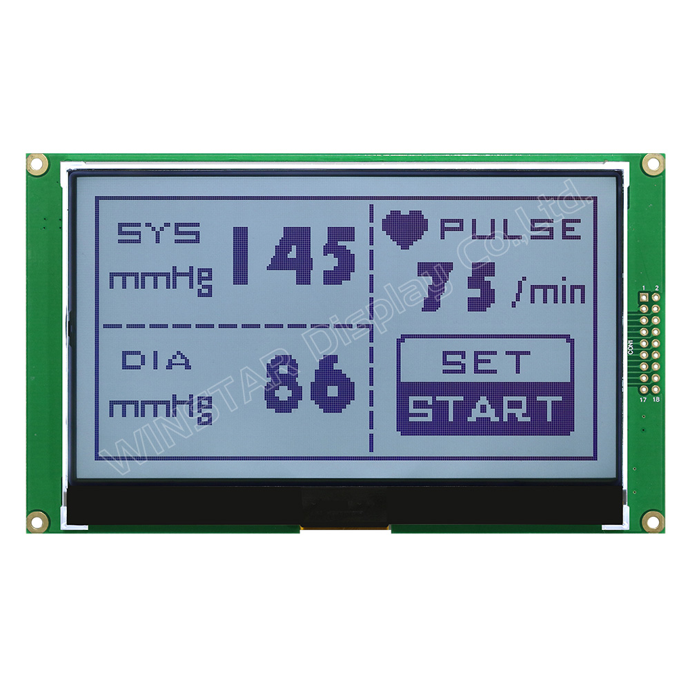
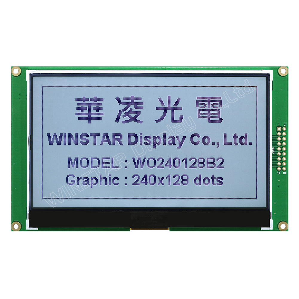
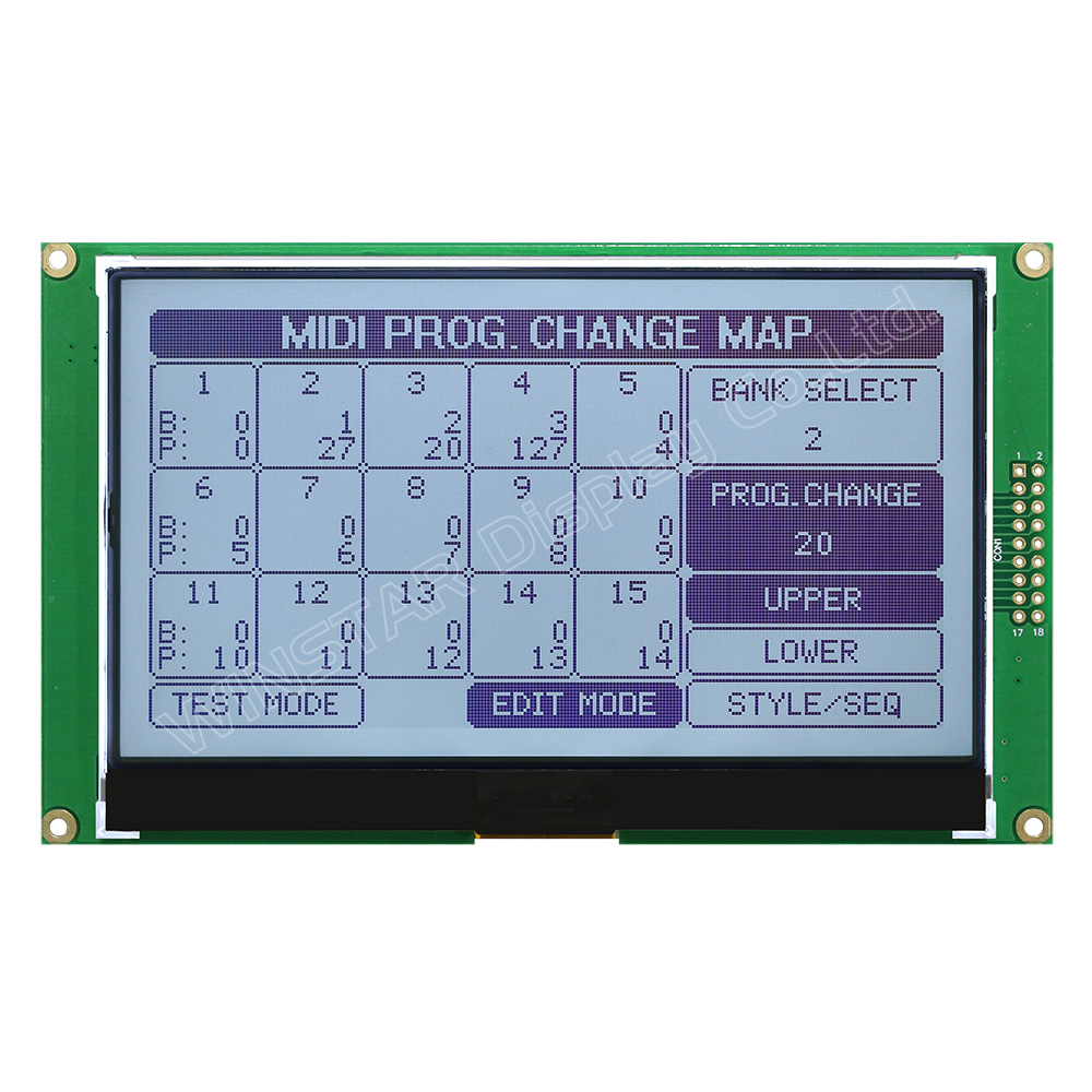

WO240128B2 是 WO240128B 4.82 吋 240x128 繪圖型 COG LCD 液晶模組的 PCB 版本,於 COG 模組上整合 PCB 板,在維持相同顯示規格的同時,可簡化安裝流程並提升系統整合便利性。搭載 ST7586S 控制器 IC,支援預設 6800 8-bit 並列介面,並提供 8080 8-bit 並列介面及 3-Line SPI、4-Line SPI 串列介面選配,採用 3.3V 邏輯電源。
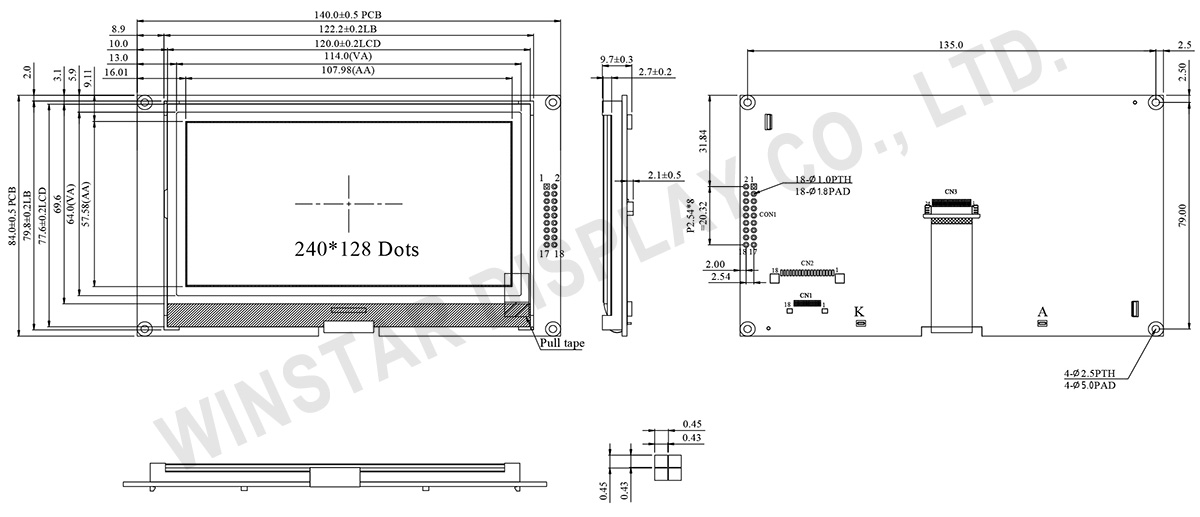
模組尺寸為 140.0 x 84.0 x 9.7 mm,檢視區域為 114.0 x 64.0 mm,有效區域為 107.98 x 57.58 mm,採用 LED 背光。
整合式 PCB 提供完整的電路配置與固定孔設計,可提升安裝便利性並簡化系統整合。提供 2.54 mm(預設)、1.0 mm 及 0.5 mm 三種連接器間距選擇,亦可選配 5V 邏輯電源版本,以符合不同系統設計需求。
提供多種 LCD 顯示模式及 LED 背光組合可供選擇,歡迎點選上方『產品詢問』,並於詢問內容中告知您的需求。
| 項目 | 標準尺寸 | 單位 |
|---|---|---|
| 點陣數 | 240 × 128 | - |
| 模組尺寸 | 140.0 × 84.0 × 9.7 | mm |
| 檢視區域 | 114.0 × 64.0 | mm |
| 有效區域 | 107.98 × 57.58 | mm |
| 點大小 | 0.43 × 0.43 | mm |
| 點間距 | 0.45 × 0.45 | mm |
| 驅動方式 | 1/128Duty,1/12Bias | |
| 背光類型 | LED | |
| IC | ST7586S | |
| 介面 | 6800 | |
| 項目 | 符號 | 最小值 | 標準值 | 最大值 | 單位 |
|---|---|---|---|---|---|
| 工作溫度 | TOP | -20 | - | +70 | ℃ |
| 儲存溫度 | TST | -30 | - | +80 | ℃ |
| LCD數位電源電壓 | VDDI | -0.3 | - | 3.6 | V |
| 類比電源電壓 | VDDA | -0.3 | - | 3.6 | V |
| LCD電源電壓 | V0-XV0 | -0.3 | - | 19 | V |
| LCD電源電壓 | VG | -0.3 | - | 5.5 | V |
| 項目 | 符號 | 條件 | 最小值 | 標準值 | 最大值 | 單位 |
|---|---|---|---|---|---|---|
| 邏輯電源電壓 | VDD-VSS | - | 3.0 | 3.3 | 3.6 | V |
| LCM電源電壓 | VOP | Ta=-20℃ Ta=25℃ Ta=+70℃ |
- 14.8 - |
- 15.0 - |
- 15.2 - |
V V V |
| 輸入高電壓 | VIH | - | 0.7VDD | - | VDD | V |
| 輸入低電壓 | VIL | - | VSS | - | 0.3 VDD | V |
| 輸出高電壓 | VOH | - | 0.8 VDD | - | VDD | V |
| 輸出低電壓 | VOL | - | VSS | - | 0.2VDD | V |
| 電源電流 | IDD | VDD=3.3V | - | 2.0 | 4.0 | mA |
| Pin No. | 符號 | 說明 |
|---|---|---|
| 1 | VDD | Power supply |
| 2 | NC | No connection |
| 3 | VSS | Ground |
| 4 | CSB | Chip select input pin CSB=“L”: This chip is selected and the MPU interface is active CSB=“H”: This chip is not selected and the MPU interface is disabled (D[7:0] are high impedance) |
| 5 | RSTB | Reset input pin. When RSTB is “L”, internal initialization procedure is executed |
| 6 | E | Read / Write control input pin. R/W = “H”: When E is “H”, data bus is in output status. R/W = “L”: The data are latched at the falling edge of the E signal. |
| 7~14 | D7~D0 | The bi-directional data bus of the MPU interface. When CSB is “H”, they are high impedance |
| 15 | R/W | Read / Write control input pin R/W = “H” : read R/W = “L” : write |
| 16 | A0 | The function of this pin is different in parallel and serial interface In parallel interface: A0 is register selection input A0 = "H": inputs on data bus are display data A0 = "L": inputs on data bus are command |
| 17 | A | LED+ |
| 18 | K | LED- |


通過點擊「允許所有 Cookie」,代表您同意在您的設備上存儲 Cookie 以增強網站瀏覽體驗、分析網站使用情況並協助我們的行銷和網站效能優化工作。您可以在我們的隱私權政策中找到有關於此的更多資訊。