

我們重視您的隱私
通過點擊「允許所有 Cookie」,代表您同意在您的設備上存儲 Cookie 以增強網站瀏覽體驗、分析網站使用情況並協助我們的行銷和網站效能優化工作。您可以在我們的隱私權政策中找到有關於此的更多資訊。


| Pin No. | 符號 | Level | 說明 | |||||||||||||||
|---|---|---|---|---|---|---|---|---|---|---|---|---|---|---|---|---|---|---|
| 1 | /CS1 | I | The chip select signal | |||||||||||||||
| 2 | /RES | I | When RES is set to “L”, the setting are initialized. | |||||||||||||||
| 3 | A0 | I | This is connect to the least significant bit of the normal MPU address bus, and it determines whether the data bits are data or command. A0 = “H”: Indicates that D0 to D7 are display data. A0 = “L”: Indicates that D0 to D7 are control data. |
|||||||||||||||
| 4 | /WR(R/W) | I | • When connected to 8080 series MPU, this pin is treated as the “/WR” signal of the 8080 MPU and is LOW-active. The signals on the data bus are latched at the rising edge of the /WR signal. • When connected to 6800 series MPU, this pin is treated as the “R/W” signal of the 6800 MPU and decides the access type : When R/W = “H”: Read. When R/W = “L”: Write. |
|||||||||||||||
| 5 | /RD(E) | I | • When connected to 8080 series MPU, this pin is treated as the “/RD” signal of the 8080 MPU and is LOW-active. The data bus is in an output status when this signal is “L”. • When connected to 6800 series MPU, this pin is treated as the “E” signal of the 6800 MPU and is HIGH-active. This is the enable clock input terminal of the 6800 Series MPU. |
|||||||||||||||
| 6~13 | D0~D7 | I/O | Data bus line | |||||||||||||||
| 14 | VDD | Power Supply |
Power supply | |||||||||||||||
| 15 | VSS | Power Supply |
Ground | |||||||||||||||
| 16 | VOUT | O | DC/DC voltage converter. Connect a capacitor between this terminal and vss or VDD | |||||||||||||||
| 17 | CAP5+ | O | DC/DC voltage converter | |||||||||||||||
| 18 | CAP3+ | |||||||||||||||||
| 19 | CAP1- | |||||||||||||||||
| 20 | CAP1+ | |||||||||||||||||
| 21 | CAP2+ | |||||||||||||||||
| 22 | CAP2- | |||||||||||||||||
| 23 | CAP4+ | |||||||||||||||||
| 24 | VRS | Power Supply |
This is the internal-output VREG power supply for the LCD power supply voltage regulator. |
|||||||||||||||
| 25 | V4 | Power Supply |
This is a multi-level power supply for the liquid crystal drive. | |||||||||||||||
| 26 | V3 | |||||||||||||||||
| 27 | V2 | |||||||||||||||||
| 28 | V1 | |||||||||||||||||
| 29 | V0 | |||||||||||||||||
| 30 | VR | I | Output voltage regulator terminal. Provides the voltage between VSS and V0 through a resistive voltage divider. IRS = “L” : the V0 voltage regulator internal resistors are not used. IRS = “H” : the V0 voltage regulator internal resistors are used. |
|||||||||||||||
| 31 | C86 | I | This is the MPU interface selection pin. C86 = “H”: 6800 Series MPU interface. C86 = “L”: 8080 Series MPU interface |
|||||||||||||||
| 32 | P/S | I | This is the parallel data input/serial data input switch terminal. P/S = “H”: Parallel data input. P/S = “L”: Serial data input. The following applies depending on the P/S status:
/RD (E) and /WR (R/W) are fixed to either “H” or “L”. With serial data input, It is impossible read data from RAM |
|||||||||||||||
| 33 | /HPM | I | This is the power control terminal for the power supply circuit for liquid crystal drive. /HPM = “H”: Normal mode /HPM = “L”: High power mode |
|||||||||||||||
| 34 | IRS | I | This terminal selects the resistors for the V0 voltage level adjustment. IRS = “H”: Use the internal resistors IRS = “L”: Do not use the internal resistors. The V0 voltage level is regulated by an external resistive voltage divider attached to the VR terminal |
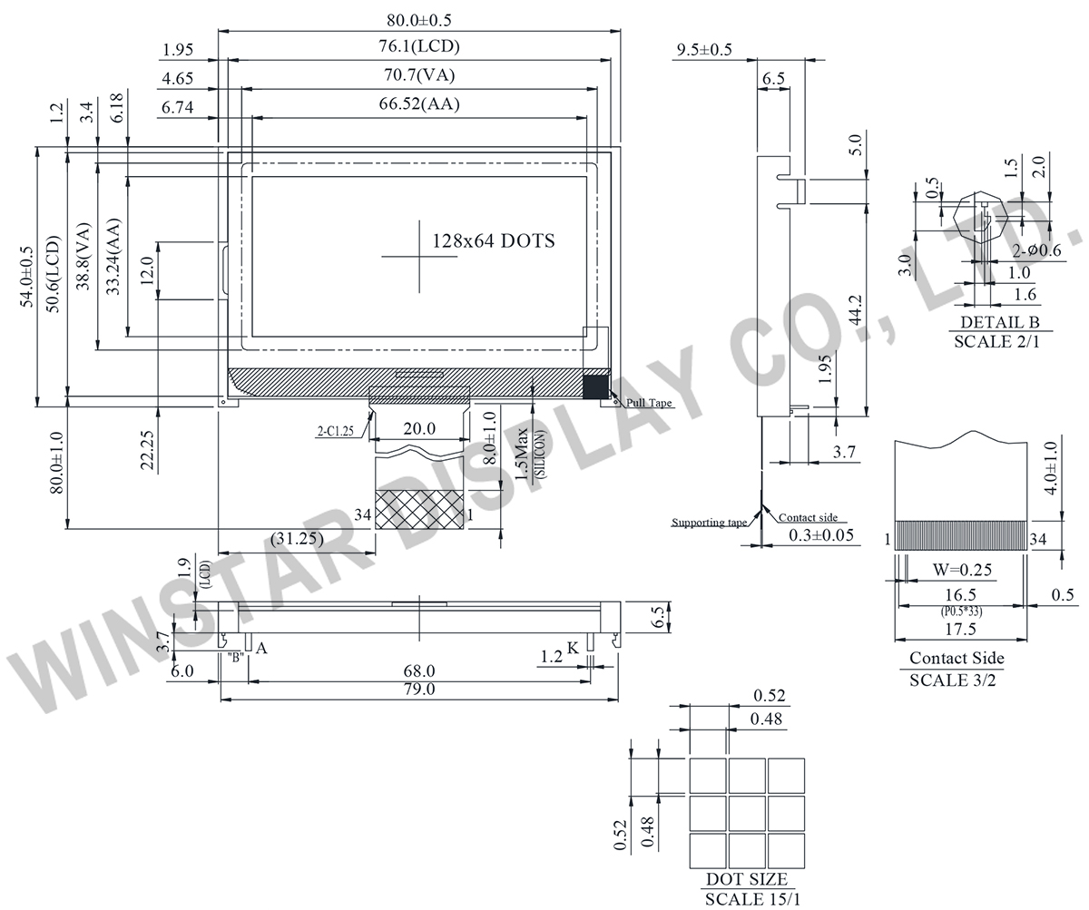
| 項目 | 標準尺寸 | 單位 |
|---|---|---|
| 點陣(解析度) | 128 x 64 | - |
| 模組尺寸 | 80.0 x 54.0 x 9.5 | mm |
| 檢視區域 | 70.7 x 38.8 | mm |
| 有效區域 | 66.52 x 33.24 | mm |
| 點大小 | 0.48 x 0.48 | mm |
| 點間距 | 0.52 x 0.52 | mm |
| 驅動方式 | 1/64 , 1/9 Bias | |
| 背光類型 | LED | |
| IC | ST7565P | |
| 介面 | 6800/8080/4-Line SPI | |
| 項目 | 符號 | 最小值 | 典型值 | 最大值 | 單位 |
|---|---|---|---|---|---|
| 工作溫度 | TOP | -20 | - | +70 | ℃ |
| 儲存溫度 | TST | -30 | - | +80 | ℃ |
| 電源電壓 | VDD | -0.3 | - | 3.6 | V |
| Power supply voltage (VDD standard) | V0,VOUT | -0.3 | - | 14.5 | V |
| Power supply voltage (VDD standard) | V1,V2,V3,V4 | -0.3 | - | V0+0.3 | V |
| 項目 | 符號 | 條件 | 最小值 | 典型值 | 最大值 | 單位 |
|---|---|---|---|---|---|---|
| 邏輯電源電壓 | VDD-VSS | - | 2.7 | - | 3.3 | V |
| LCM電源電壓 | V0-VSS | Ta=-20℃ Ta=25℃ Ta=70℃ |
10.0 9.8 9.6 |
10.2 10.0 9.8 |
10.4 10.2 10.0 |
V V V |
| 輸入高電壓 | VIH | - | 0.8 VDD | - | VDD | V |
| 輸入低電壓 | VIL | - | VSS | - | 0.2VDD | V |
| 輸出高電壓 | VOH | - | 0.8VDD | - | VDD | V |
| 輸出低電壓 | VOL | - | VSS | - | 0.2VDD | V |
| 電源電流(不包括LED背光) | IDD | - | - | 0.6 | 1.0 | mA |

通過點擊「允許所有 Cookie」,代表您同意在您的設備上存儲 Cookie 以增強網站瀏覽體驗、分析網站使用情況並協助我們的行銷和網站效能優化工作。您可以在我們的隱私權政策中找到有關於此的更多資訊。