我们重视您的隐私
通过点击「允许所有 Cookie」,代表您同意在您的设备上存储 Cookie 以增强网站浏览体验、分析网站使用情况并协助我们的营销和网站效能优化工作。您可以在我们的隐私权政策中找到有关于此的更多信息。

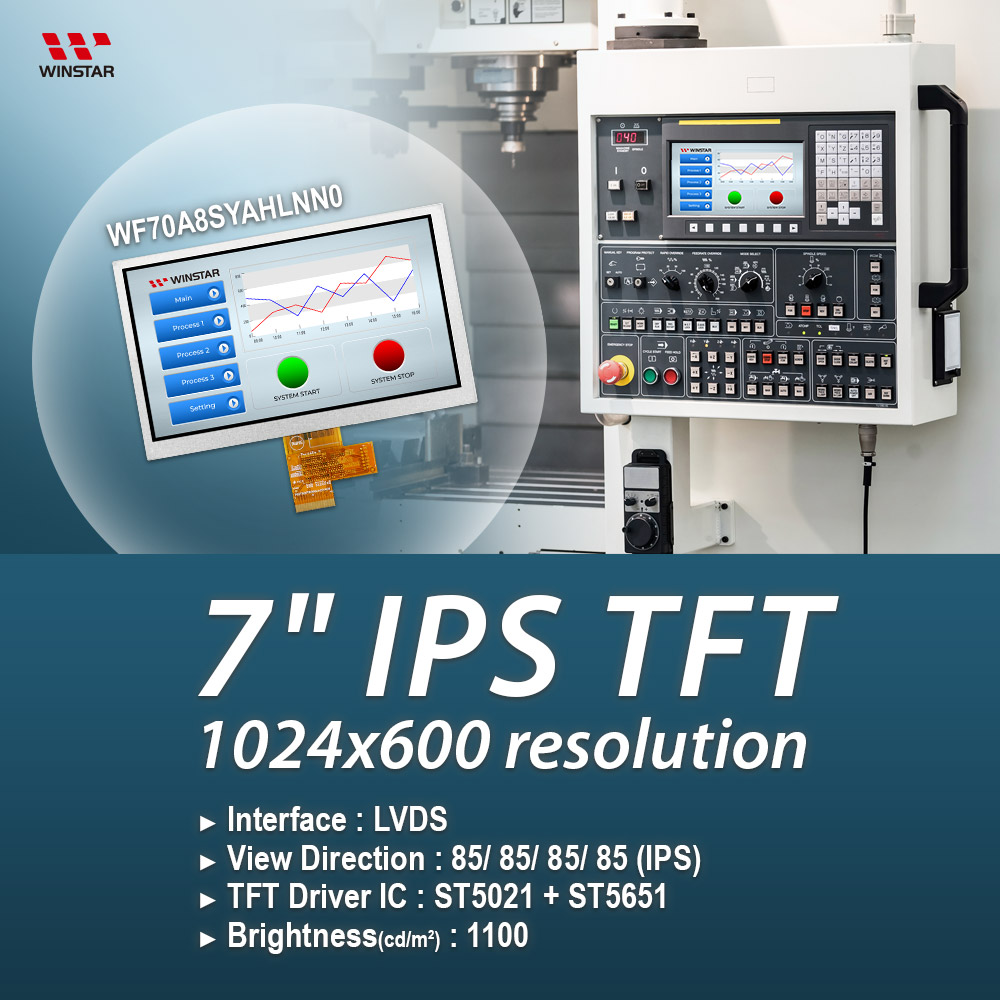
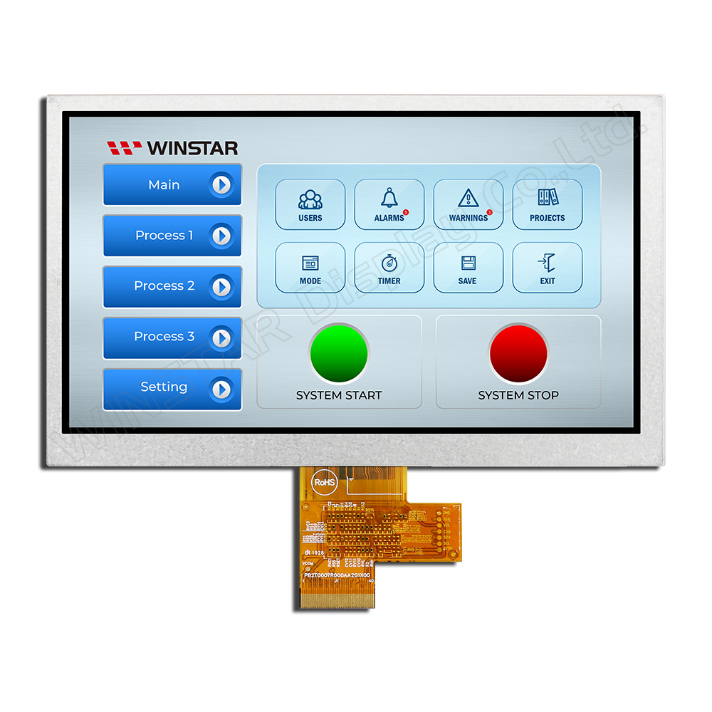
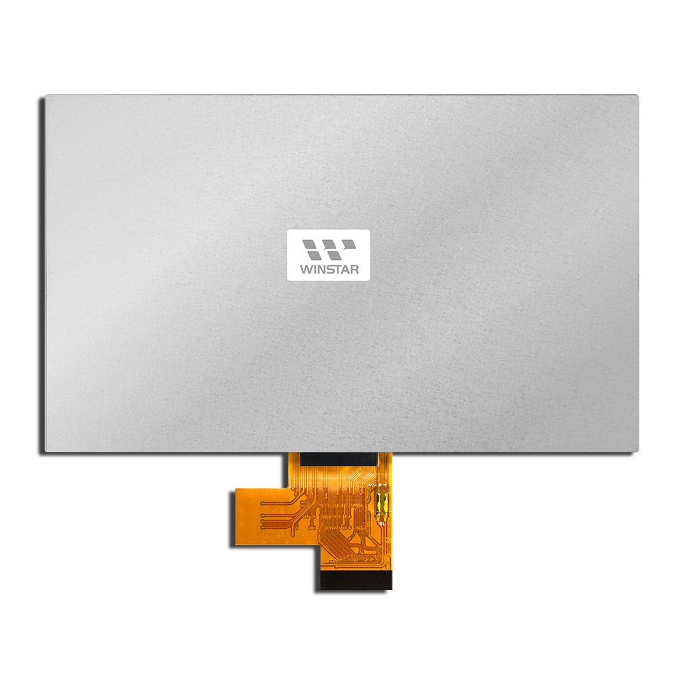
WF70A8SYAHLNN0 是一款 7英寸高亮 IPS TFT 液晶显示屏,分辨率为 1024x600,屏幕比例为 16:9。该型号采用 ST5021 和 ST5651 驱动 IC,支持 LVDS 接口。
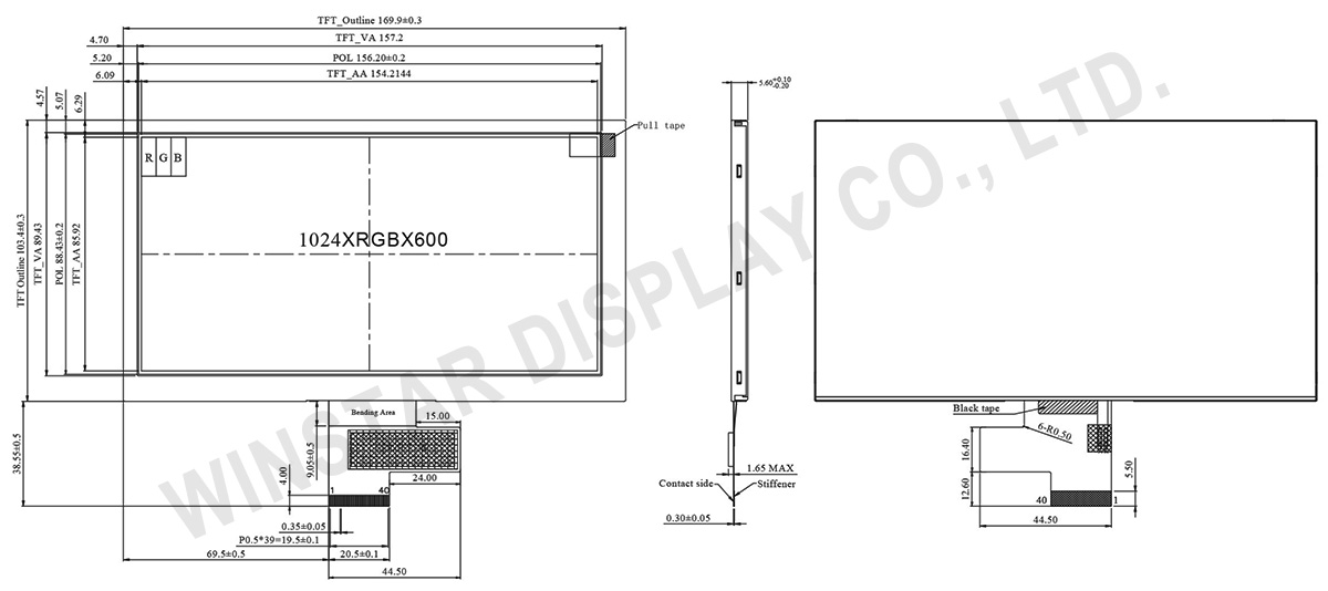
显示屏典型亮度为 1100 cd/m²,对比度为 800:1,采用 Normally Black 透射式 LCD,表面经过防眩光(Anti-Glare)处理。IPS 面板提供 85/85/85/85(典型值)的宽视角。模组尺寸为 169.9 x 103.4 x 5.6 mm,有效显示区域(AA)为 154.2144 x 85.92 mm。
电源电压(VDD)范围为 3.0V 至 3.6V,典型值为 3.3V。工作温度范围为 -20°C 至 +70°C,储存温度范围为 -30°C 至 +80°C。
| 项目 | 规格 | 单位 |
|---|---|---|
| 尺寸(对角线) | 7 | 寸 |
| 点阵(分辨率) | 1024 × RGB × 600(TFT) | dots |
| 模块尺寸 | 169.9(W) × 103.4(H) × 5.6(D) | mm |
| 有效区域 | 154.2144 × 85.92 | mm |
| 点间距 | 0.1506 × 0.1432 | mm |
| LCD类型 | TFT, 平常黑, 透射式 | |
| 视角 | 85/85/85/85 | |
| 长宽比 | 16:9 | |
| TFT 驱动 IC | ST5021 + ST5651或相容IC | |
| 背光类型 | LED, 平常白 | |
| 触控面板 | 无触控面板 | |
| TFT 接口 | LVDS | |
| 表面 | 防眩光 | |
| 项目 | 符号 | 最小值 | 典型值 | 最大值 | 单位 |
|---|---|---|---|---|---|
| 工作温度 | TOP | -20 | - | +70 | ℃ |
| 储存温度 | TST | -30 | - | +80 | ℃ |
| 项目 | 符号 | 标准值 | 单位 | ||
|---|---|---|---|---|---|
| 最小值 | 典型值 | 最大值 | |||
| 电源电压 | VDD | 3.0 | 3.3 | 3.6 | V |
| 类比电源电压 | AVDD | 8.9 | 9.0 | 9.1 | V |
| TFT Gate ON 电压 | VGH | 17 | 18 | 19 | V |
| TFT Gate OFF 电压 | VGL | -6.5 | -6.0 | -5.5 | V |
| TFT Common 电压 | Vcom | 3.0 | 3.15 | 3.3 | V |
| 驱动电流 | IDD | - | 14 | 21 | mA |
| 电源电流 | IAVDD | - | 25 | - | mA |
| TFT Gate ON 电流 | IVGH | - | 1 | - | mA |
| TFT Gate OFF 电流 | IVGL | - | 1 | - | mA |
| TFT Common 电流 | IVCOM | - | 1 | - | mA |
LCM PIN 定义
| Pin No. | 符号 | I/O | 功能说明 |
|---|---|---|---|
| 1 | VCOM | P | Common Voltage |
| 2 | VDD | P | Digital circuit |
| 3 | VDD | P | Digital circuit |
| 4 | NC | --- | No connection |
| 5 | RESET | I | Global reset pin |
| 6 | STBYB | I | Standby mode, Normally pulled high STBYB = “1”, normal operation STBYB = “0”, timing controller, source driver will turn off, all output are High-Z |
| 7 | GND | P | Ground |
| 8 | RXIN0- | I | Negative LVDS differential data input |
| 9 | RXIN0+ | I | Positive LVDS differential data input |
| 10 | GND | P | Ground |
| 11 | RXIN1- | I | Negative LVDS differential data input |
| 12 | RXIN1+ | I | Positive LVDS differential data input |
| 13 | GND | P | Ground |
| 14 | RXIN2- | I | Negative LVDS differential data input |
| 15 | RXIN2+ | I | Positive LVDS differential data input |
| 16 | GND | P | Ground |
| 17 | RXCLKIN- | I | Negative LVDS differential clock input |
| 18 | RXCLKIN+ | I | Positive LVDS differential clock input |
| 19 | GND | P | Ground |
| 20 | RXIN3- | I | Negative LVDS differential data input |
| 21 | RXIN3+ | I | Positive LVDS differential data input |
| 22 | GND | P | Ground |
| 23 | NC | --- | No connection |
| 24 | NC | --- | No connection |
| 25 | GND | P | Ground |
| 26 | NC | --- | No connection |
| 27 | NC | --- | No connection |
| 28 | SELB | I | 6bit/8bit mode select H:6bit / L:8bit |
| 29 | AVDD | P | Power for Analog Circuit |
| 30 | GND | P | Ground |
| 31 | LED- | P | LED Cathode |
| 32 | LED- | P | LED Cathode |
| 33 | L/R | I | Horizontal inversion |
| 34 | U/D | I | Vertical inversion |
| 35 | VGL | P | Negative power for TFT |
| 36 | NC | --- | No connection |
| 37 | NC | --- | No connection |
| 38 | VGH | P | Positive power for TFT |
| 39 | LED+ | P | LED Anode |
| 40 | LED+ | P | LED Anode |
I:input ,O:output,P:power


通过点击「允许所有 Cookie」,代表您同意在您的设备上存储 Cookie 以增强网站浏览体验、分析网站使用情况并协助我们的营销和网站效能优化工作。您可以在我们的隐私权政策中找到有关于此的更多信息。